

CometCAD is a tool for creating circuit schematics and printed circuit boards (PCBs). With the tiny green board inside every electronic system deciding the complete functionality of the system, creating worthy designs take priority. With this thought in mind, this month we explore designing a PCB using CometCAD.
CometCAD is built for Windows and falls under free-use licence. Design of the PCB using this software is divided into three stages: symbols, circuit and layout. Let us take a look at how each of these translate to the expected end design we are looking for. To begin with, we have a few notable features.
Look at your drawings how you want
As you work with CometCAD, you have the option to customise the settings of the screen. You might be working on a tiny-screen laptop or a wide-screen desktop, but when dealing with design, the correct zoom and optimum aspect ratio turn out to be as important as the design itself. You also have the liberty to configure the workspace for your circuit, right from the size of the sheet to spacing and visibility of grid lines.

Leave behind a footprint
A footprint is a pattern describing the arrangement of  pads or through-holes used to physically attach and electrically connect the components to a PCB. Effectively, it is similar to the map of the components on the board. With CometCAD, symbols can be linked to footprints, while off-page connectors can contain footprints other than for those that work as signal connectors.
The connectors then refer to the footprint for their pin configuration, which can be accessed individually, or the total number of pins can be split between sheets. Once created, symbols and footprints are stored in the library for further use. These are termed parts and can simply be added to the circuit like any ordinary symbol.
Fit in your PCB anywhere, anyhow
Often we see PCBs fitted onto other boards with nails or screws. Holes for these can be added in the design stage itself, via the tool. But the allowed size of the hole is fixed. If holes of other dimensions are needed, at design stage you can add a polygon around the region, so as not to route traces through that area. This is called a cut-out and can be milled in the final stage.
Architecting the board
You can choose to create a new PCB layout from scratch or update an existing PCB file, which is called forward annotation. Every PCB layout requires a circuit schematic as an input, and on importing the same, CometCAD allows you to estimate the area of the final PCB.
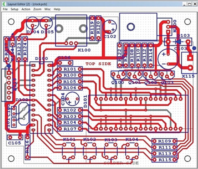
The layout editor allows you to edit the different layers of the PCB. The tool provides a polygon function, which can be used to set the borderline for your board and include gaps or cuts and copper planes on the PCB. These parameters will decide the fill rate area for the PCB. In other words, these will decide the area of the PCB that is available for the parts to be placed.
For making a selection, say a footprint, the layer you choose is the active layer. Setting the active layer is in your hands. You can also change the width of a trace along the PCB, although it cannot be smaller than that specified in the rules. You can add parallel traces to change a specific route and also divide a trace into new segments.
Vias, which provide contact between metals of different layers, cannot be moved once connected. While a trace can run from the pad of a footprint to a via, an unconnected via cannot have a trace connecting it to a pad.
Find with ease. It is always difficult to identify specific components once the design is almost complete, thanks to the mess of traces and layers. A well-managed find option here lets you zoom to the exact point you are looking for, be it a node, a signal or a certain resistor. This shows up along with the traces connected to it, making it easy for you to debug.
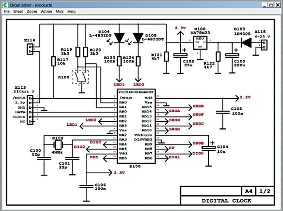
Putting together a circuit
It is, of course, the circuit schematic that decides how your setup functions. The schematic is created on a user-specified sheet frame, and each  action performed is considered as a function by the tool. General basic options like create, move, mirror and rotate can be accessed by the given menus or shortcut keys. Each component can be configured according to your needs and can be appropriately named.
Complex designs like a communication interface demand a bus, which is a simple graphics item on the tool, but connections will have to be made manually. While moving a symbol does not automatically move the wires connected to it, a function called fix wires can be exploited to help with this aspect. The function can not only remove unwanted wires but can also split wires into segments that can be selected separately. The tool can even generate rectangular wire corners wherever specified.
Creating the basic element, a symbol
A symbol editor takes care of your requirements for creating the symbols that make up your design. A symbol could be an ordinary, graphics or connector type. While regular connection of wires is the norm, graphics symbols take care of graphics and even text that you may want to include in your circuit. With an automatic check of every pin number you enter for the symbols, any number that is missed out is flagged to the user immediately.
Configurable connectors aid achieving connection between different parts of the design. While it is not uncommon to have a design spanning more than a single sheet, CometCAD provides off-page connectors to establish continuity between pages.
An error check to be sure
Every PCB design is based on specifications given by the manufacturer, and the design you create is put through an error check. At this stage, the design and all its connections are cross-checked against the rule file given by the manufacturer, and errors are identified.
CometCAD does not allow you to generate the output file until and unless the design undergoes a check. Outputs created are all computer-aided manufacturing (CAM) files. Gerber and mill files are also created, along with required reports. Depending on the type of PCB panel selected, the PCB borderline and PCB area overlap is selected.
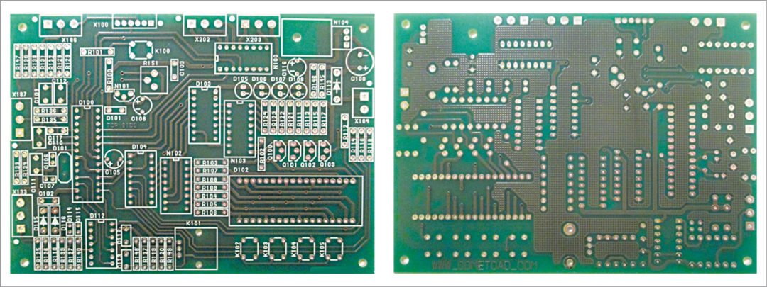
This completes our journey from symbols to layout. Go ahead and get your PCB made. You can even create a double-side PCB or a dual-layer PCB. Your very own hardware is just weeks away!
Download latest version of the software
Priya Ravindran is a freelance writer with EFY


Hi I have a query is it possible to develop RF transmitter (ADF7012) using cametCAD tool?
Please elaborate your query.
Wish to know the purchase price of this utility
You can get all the information here