
Introduction

The embedded systems should drive different peripheral devices requiring significant electrical power.
A typical case is the DC motors, operating from 6V, 12V and 24V.
These motors may require up to 3A average current and much more peak current.
It is safer and cheaper to use transistorized drivers for these purposes.
Power transistors are cheap, more difficult to damage and easier to replace if damaged compared to the most integrated circuits – drivers with the same parameters.

That short paper is presented dual universal hardware driver for embedded systems with many applications.
The circuit can be controlled by TTL/CMOS signals produced by most of the MCUs, MPUs and peripheral integrated circuits.
Description of the circuit
Figure 1 is showing the circuit of dual universal hardware driver for embedded systems.
The circuit has two identical channels built around Darlington transistors T1 to T4.

We may use large variety of transistors, e.g. TIP122 and TIP127.
Also we may use ordinary bipolar transistors as BD135/BD136, TIP41/42, etc but the maximal output current is limited to around 0.5A.
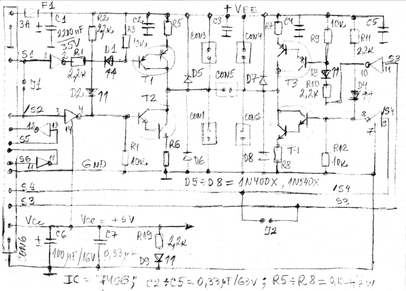
Both channels of the driver can work independently, in parallel and in bridge configuration.
The driver has five output connectors CON1 to CON5 and they can be used to drive large variety of loads.
The input control signals for the dual driver are S1, /S2, S3 and /S4.
The signal S1 is controlling the transistor T1, /S2 is controlling transistor T2, S3 is controlling transistor T3, and /S4 is controlling transistor T4.
The active levels of S1 and S3 are HIGH and the active levels of /S2 and /S4 are LOW!
The LEDs D1 to D4 are showing the status of the control signals and the transitors.
The LED1 is ON when the transistor T1 is ON.
The LED2 is ON when the transistor T2 is ON.
The LED3 is ON when the transistor T3 is ON.
The LED4 is ON when the transistor T4 is ON.
There is no limit for the lowest frequency of switching the transistors T1 to T4.
We may do the control manually with electrical switches controlling S1 to S4.
The maximal switching frequency is limited by transistors and the loads and can be more than 20kHz.
Cautions
We may use 7407 instead on 7406 but in that case the active levels of the control signals will be inverted.
Both circuits are with open collectors at the outputs.
With appropriate Darlington transistors we may obtain output current to more than 10A, but it is strongly recommended to limit the output current up to around 3-5A.
It is recommended to use Fuse F1 for maximum 3A.
Also we should make appropriate conductors on the pcb in order to meet large currents.
The filtering capacitors C1 to C6 should not be omitted.
C1 should be at least 470uF per Ampere.
C2 to C5 are from 0.15 to 0.47uF/63V.
We may connect loads to ANY combination of the output connectors CON1 to CON5 under the condition that the transistors are not overloaded and the algorithm of the controlling these loads is appropriate.
Jumpers J1 and J2 are giving the possibility to control the driver with just two signals.
It is not recommended to use these jumpers at high frequencies and high loads.
In most of the cases for the optimal and safe control we should use all four signals and the jumpers should be open, e.g. in many cases we are need to obtain “dead time” for the control pulses.
During that “dead time” all transistors are OFF!
Again transistors T1 and T2 and transistors T3 and T4 should never be ON in the same time!
Resistors R5 to R8 are obligatory.
They are in the range from 0.1Ohm to 0.47Ohm and with power dissipation at least 2W.
The power supply
The connector CON6 is for the power supply and the control signals in the same time.
The driver has two power supplies Vcc and +Vee.
Vcc is the standard power supply for 7406 or 7407 or Vcc = 5V+-5%.
+Vee is the peripheral power supply.
It can be anywhere between 6V and 30V, preferably above 10V.
It should be noted that the maximal power supply for the open collector of 7406/7407 is 30V.
Vee is protected with fuse F1.
The fuse F1 should be fast and for appropriate current ratings.
The driver can work with 12V and 24V rechargeable batteries.
Heat sinks
Transistors T1, T2, T3 and T4 should be obligatory mounted on appropriate heat sinks according to the targeted applications.
T1 and T2 can be mounted on common heat sink without insulations because usually the metallic part of the package is connected with the collectors.
T3 and T4 also can be mounted on common heat sink.
If we use two separate heat sinks for T1+T2 and T3+T4 they should be with thermal resistance below 15C/W.
If we use common heat sink for all four transistors it should be with thermal resistance below 10C/W.
The size of the heat sinks depends on the loads and the power supply.
In practice we should keep attention at least for the following:
1/ The frequency of the switching should be appropriate.
If the frequency is too high the transistors can overheat.
2/ When possible the temperature of the transistors should be monitored.
3/ When possible we should have additional over current protection in the power supply.
4/ At high currents and high switching frequencies we may add small cooling fan, e.g. 12V/0.1-0.2A
5/ We should use R5 to R8 to monitor the current of the transistors.
Conclusions
That short paper is presenting dual universal hardware driver for embedded systems
The circuit may drive DC motors, incandescent bulbs, relays, loudspeakers, transformers, solenoids, inductors, LEDs, long cables, etc. but we should take considerations about the parameters of the loads and the implementation of the driver.
The control inputs S1, /S2, S3 and /S4 are TTL and CMOS compatible for control system working with 5V.
They can be driven directly from most of the MCUs.
There are two free inverters in 7406 and we may use them to obtain active LOW levels for the signals S1 and S3 or active HIGH levels for the signals /S2 and /S4 or for any other appropriate goals.


