
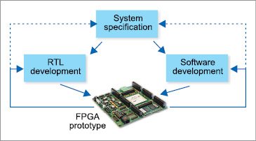
Field programmable gate array (FPGA) prototyping, commonly referred to as FPGA based prototyping, application-specific integrated circuit (ASIC) prototyping or system on chip (SoC) prototyping, is the method to prototype SoC and ASIC designs on FPGAs for hardware verification and early software development.
FPGA is a much faster engine for running the register transfer level (RTL) model. Running an SoC design on an FPGA prototype is a reliable way to ensure that it is functionally correct. About a third of all current SoC designs are fault-free during their first silicon pass, with nearly half of all re-spins caused by functional logic errors. FPGA based prototyping allows speed ranges into tens of MHz and often offers the best cost-per-gate per MHz for software development and hardware regressions in the project phase when RTL becomes stable enough, so that fast turnaround time and hardware debug matter less.
A single prototyping platform can provide verification for hardware, firmware and application software design functionality before the first silicon pastime-to-market (TTM) period is shrinking. It is typically limited in capacity and can take months to bring up due to modifications required in the design and subsequent verification. The benefit, once brought up, is a speed range in tens of MHz range that is sufficient for software development.
In today’s technological-driven society, new products are introduced rapidly, and failing to have a product ready at a given market window can cost a company a considerable amount of revenue. If a product is released too late, the product could be rendered useless, costing the company its investment capital for the product.
After the design process, FPGAs are ready for production, while standard-cell ASICs take more than six months to reach production. Today, state-of-the-art ASIC prototyping and software development tools join software development platforms running reference designs with pre-packaged IP configurations. Prototyping kits are operational out-of-the-box, and allow hardware and software developers to immediately engage in integration and validation tasks necessary to ship the next great SoC design.

With the increasing cost of mask sets and continuous decrease of IC size, minimising the number of re-spins is vital to the development process. Single FPGA devices can hold up to 20 million ASIC gates, with utilisation rates of 60 per cent and FPGA systems promise to hold almost 100 MGs. Earlier, the most common hardware configuration on the FPGA prototyping board consisted between four to nine clocks, with the fastest clock running more than 200MHz.
Key advantages and issues
Prototyping is important because of high performance and accuracy, real-time dataflow and extended RTL testing and debugging. FPGA based prototypes offer unbeatable flexibility, capacity and speed. The key advantage of FPGA based systems is speed and the main volume of FPGA based prototypes today is to enable software development and sub-system validation. Many benefits come from the co-design of prototype hardware, firmware and software elements that help expedite migration from raw ASIC RTL and IP.
From a chip perspective, at about 60 per cent into a project, three main issues have to be resolved. First, error rate in the hardware has to be low enough that design teams find confidence to commit to a tape out.

Second, the chip has to be validated enough within its environment so that it works within the system.
The last is that, significant portions of the software have to be brought up to be confident that software/hardware interactions work correctly.
Abstraction levels
Prototyping today happens at two abstraction levels, namely, using transaction-level models (TLMs) and register transfer level (RTL) models, using five basic engines.
1. Virtual prototyping based on TLM models
2. RTL simulation
3. Emulation
4. FPGA based prototyping
5. Bringing up
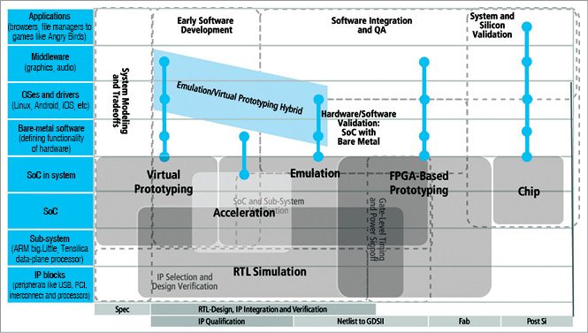
FPGA basic engines
FPGA based emulators are typically weaker with respect to debug efficiency and turnaround time, making these less reactive and similar to FPGA based prototypes. The downside to standard FPGA based prototyping is capacity limitations as well as longer bring-up due to the changes that have to be made to map the RTL to the FPGAs. So only the efficient combination of the four engines, namely, emulation, virtual prototyping, RTL simulation and FPGA based prototyping, provides a complete solution.
Emulation. Emulation extends verification to the full chip and at the chip-in-system level by enabling connections to real system environments like PCI, USB and Ethernet. The main advantage of processor based emulation is fast turnaround time for bring-up, which makes it ideal for the project phase in which RTL is not quite mature yet.


