
Design Guidelines for switching regulators
Efficiency is an important parameter to judge the system performance. Efficiency can be improved by reducing the losses. The main source of losses for switching regulators are conduction and switching loss in the upper MOSFET, conduction loss in the channel and body diode of bottom MOSFET, conduction and magnetic loss in the inductor, loss in the filter capacitors.
- Conduction loss in the MOSFET depends upon the on-state resistance (Ron) value and the current flowing through the device.

MOSFET static model (a) turn on, (b) turn off On state resistance is proportional to the blocking voltage of the MOSFET. The blocking voltage of the MOSFET is decided based on DC bus voltage. Designer always choose the device with blocking voltage rating higher than the DC bus voltage. This is because of two reasons mainly: there is an overvoltage across the switch during turn off and designer always deigns with some factor of safety. But there should not be a high percentage of factor of safety. It will increase the conduction loss.
- Switching loss in upper MOSFET happens during switching transitions (switching on and switching off transitions) as the MOSFET switching is not ideal.
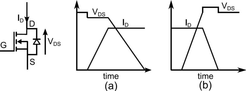 This loss is proportional to the switching frequency, instantaneous current trough the device and the voltage across the device during the off-state condition. The parasitic capacitance values change proportionally with the voltage and current rating of the device. So, the switching loss will increase. On state resistance drops when a high current MOSFET is selected. But it will increase the switching loss. So, there should be an optimum value which needs to be decided by the designer.
 - As soon as the upper MOSFET is turned off, inductor current starts to freewheel through the body diode of the bottom MOSFET. A dead-time is provided in between the switching of two MOSFETs to avoid cross conduction. During dead-time, inductor current fully flows through the body diode. As it is not optimized for conduction loss, a large amount of power loss occurs here. So, dead time value should not be too low such that cross conduction happens. From the other angle, it should not be too high, otherwise it ends up with bad system efficiency.
- After the dead-time, bottom MOSFET is gated, channel takes over most of the current flowing through the body diode and power loss reduces.
- Conduction loss happens in the induction mostly because of its DCR. Increasing the cross-sectional area of the conductor reduces the DCR value. But it will increase the size of the inductor. There is another component of loss in the inductor comes from magnetic loss when iron core inductors are used. Air core inductors are free from magnetic loss and used for switching regulators with higher switching frequency.
- The output capacitive filter is not ideal and it has some ESR. There will be small amount of power loss occurs there. Capacitor with very low ESR must be selected to get a good efficiency.
- The system efficiency for light load condition is very low when only pulse width modulation (PWM) is used. So, for light load condition regulator can be switched to pulse frequency modulation (PFM) for better efficiency.
- Switching frequency decides the filter size. Higher switching frequency reduces the filter size and simultaneously the losses in the filter. But it increases switching losses and requires larger board size or heat sink to dissipate the heat generated. It also reduces the system efficiency. So, the switching frequency selection is a tough job for the designer and needs to be selected judiciously to get the optimum performance out of the regulator. Generally, for point of load regulator typical switching frequency ranging from 100 kHz to 1 or 2 MHz.
- For a constant switching frequency, smaller inductance gives larger ripple and larger RMS current on the MOSFET. This increases the conduction loss in the upper MOSFET. On the other hand, high inductance gives larger inductor size and higher DCR value. Generally, 10-60% current ripple is permissible and selected depends upon the application.
- The inductor in any switching regulator topology acts as a constant current source. When the MOSFET switches, depending upon the topology, there will be pulsating switching current in the input or output or both. i.e. for buck topology there will be pulsating switching current flowing in the input. So, the input capacitor sees very high ripple current. So, capacitor with very low ESR must be selected as the RMS current is high. As the switching current is flowing through the input capacitor and the MOSFET for buck topology, input capacitor should have a very low ESL value and it should be placed very close to the power MOSFETs. The input capacitor should have some high frequency ceramic capacitors (most likely X5R or X7R) in parallel with bulk ceramic or electrolytic capacitors such that impedance over wide frequency range should be low.
For buck topology, the output current is continuous. But it is not constant current, there is ripple in it. AC part of this current is flowing through the output capacitor. So, to reduce the output ripple voltage, ESR and ESL of output capacitor needs to be low. So, output capacitor should also have some high frequency ceramic capacitors in parallel with bulk ceramic or electrolytic capacitors such that overall ESR and ESL value is low. For boost and buck-boost topologies, the output current is switching pulsating current. So, capacitor selection demands special attention.
- Good transient performance in supply system is always required for embedded applications. For faster response against load transient and input voltage disturbance, system bandwidth should be high. But system bandwidth is restricted by the switching frequency. Generally, system bandwidth should be at least one fifth times of switching frequency. Selection of higher switching frequency helps in faster transient response. Transfer function of buck topology is fairly simple. It has double pole at LC oscillation frequency and a zero added by output filter in conjunction with capacitor ESR. A compensator network needs to be designed properly to get proper gain and phase margins. A lower phase margin leads to oscillation whereas a high value of phase margin makes the system response slower. Phase margin needs to be something around 30-45 degree for proper operation. For boost and buck-boost topologies, there is a right-hand side zero in the transfer function which will give phase loss and may cause instability for light load conditions. Special attention needs to be paid during the design of compensators for such regulators.
- Switching transition may cause EMI problems if the transition time is too low. By increasing the value of gate resistance of the MOSFETs, transition times can be increased and ultimately it reduces EMI. Though the bad part is it increases switching loss.

Hlo
I actually need to design a power supply of 12v,53a.
Can you please help me.
muy bueno muchas gracias por compartir
Gracias por tus comentarios