


In recent years switched capacitor circuit has gained popularity due to their suitability in integrated circuits.
The two major problems faced by IC designers are:
1. Implementing a large-value resistor requires a large chip area.
2. Difficulty arises in designing RC active circuits having precise time constants.
Switched Capacitor Principle
In a switched capacitor circuit both these difficulties are circumvented by simulating a resistor with a capacitor that occupies smaller chip area. Also time constant is made to depend on a highly stable crystal oscillator frequency and ratioed capacitors.
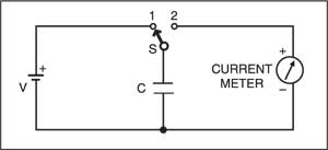
The basic principle of simulating a resistor with a switched capacitor is shown in Fig. 1.
Suppose initially the SPDT switch (S) connects the capacitor (C) to the voltage (V) at contact 1. The charge (Q) acquired by the capacitor is:
Q = C .V … …(1)
If the switch is now shifted to contact 2, the capacitor discharges fully and the charge of the capacitor passes to the ground.
If the switch is moved back and forth very rapidly with frequency f or time period T (=1/f), the average current flowing through the current meter will be:
I=C .V/ T … …(2)
or,
V/I = 1/C.f … (3)
From Eq.(3), it’s clear that the switched capacitor simulates a resistor (R) given by:
R= 1/ C.f … …(4)
As switching cannot be done manually, you require an electronic switch. IC CD4066 (IC1) includes four such CMOS bidirectional analogue switches in a single package. An electronic switch has a control terminal apart from two input/output (I/O) terminals. The enable input pins (pins 5 and 13) are driven by a unipolar square wave (clock) having two discrete voltage levels. When control is at logic 0 (0V) the switch is open, and when the control is at logic 1 (12V) the switch is closed. Using two such switches you can build the required SPDT switch as shown in Fig. 2. When one switch is closed, the other has to be kept open, and vice versa. That means you must drive the two control terminals by complementary clocks.
Switched Capacitor Circuit
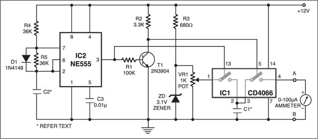
Timer IC NE555 (IC2) is operated in astable mode to generate the square wave. The 50% duty cycle is achieved by equal-value timing resistors (R4=R5) and diode D1. The inverting (NOT) operation is performed traditionally by transistor T1 (2N3904) to generate the complementary clock. A frequency meter can read out the actual frequency.
Construction & testing
You should perform the experiment on a breadboard. Connect a suitable capacitor (C2) for generating the required test frequency between pin 2 of IC2 (NE555) and ground. Connect test capacitor C1 (preferably mylar or teflon capacitor) between pin 2 (joined to pin 3) of IC1 and ground.
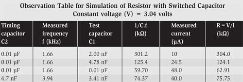
Adjust trimpot VR1 to 3 volts. This voltage is applied to pin 1 of IC1. Connect the test capacitor (C1) and note the frequency and current readings on the frequency meter and the microammeter, respectively. Calculate resistance (R) from the relationship:
R=V/I
Now check whether this value satisfies Eq.(4).
Record observations for various combinations of f and C in the form of a table.
Finite values of the ‘on’ resistance of analogue switches (approx. 80 ohms) and microammeter resistance (typically 1-2 kilo-ohms) will be all swamped out if you simulate a high-value resistor.
The article was first published in December 2003 and has recently been updated.
