
Audio noise can be annoying, especially if you are trying to listen to a very weak radio station. Peaks of unwanted background noise completely swamp the broadcast signal, making it unintelligible. The audio noise limiter circuit presented here overcomes this problem by limiting the noise peaks. It can be used with AM short-wave (SW) receivers and amateur radio (HAM) transceivers.
Audio noise limiter circuit
Fig. 1 shows the circuit diagram of the audio noise limiter. It is built around TL072 (IC1) and a few other components. TL072 contains two high-speed junction gate field-effect transistor (JFET) input operational amplifiers (A1 and A2).
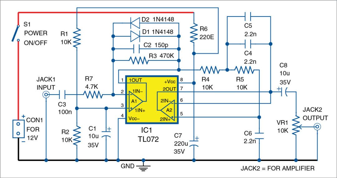
Both the noise and the audio signal are fed to the inverting input of A1 (pin 2) in IC1 via capacitor C3. The operational amplifier (or op-amp) is biased by resistors R1 and R2 to half the supply voltage. Its gain is around 100, which helps in buffering the audio signal. Diodes D1 and D2 conduct on noise peaks and limit its peak-to-peak swing to about 1.2 volts.
The next stage is built around op-amp A2. It forms a  Sallen-Key Butterworth active low-pass filter. Its cut-off frequency of 5kHz is determined by capacitors C4, C5 and C6. It restricts the audio response and filters out unwanted noise by attenuating frequencies higher than 5kHz. Resistor R6 and capacitor C7 give a clean supply voltage to the op-amps.
Output from potmeter VR1 can be used to drive LM386 or TDA2003 audio amplifier chips. This greatly reduces the noise.

Changing values of capacitors C4, C5 and C6 to 4.7nF will limit the audio bandwidth to 2.5kHz and further reduce the noise. Due to 4.7k (R7) resistor between C3 and pin 2 of TL072, audio gain will be R3/R7 = 470k/4.7k = 100 or 20dB.
The circuit is not designed for use with mobile phones. It is designed for use in SW and HAM receivers, and that too only for voice. It is basically a low-pass filter that filters out background noise and makes the speech more intelligible since human speech falls mostly in the range of 300Hz to 3.5kHz.
Connect JACK1 to audio output of a SW receiver and JACK2 to any audio amplifier circuit. Noise is reduced due to the active low-pass filter formed around the op-amp. It attenuates all frequencies above 5kHz.

Construction and testing
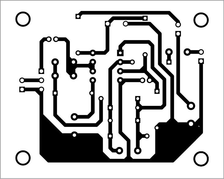
A single-side PCB for the audio noise limiter is shown in Fig. 2 and its component layout in Fig. 3. After assembling the circuit on the PCB, enclose it in a suitable plastic box.
Keep all leads as short as possible. Connect the SW radio receiver output to JACK1 and output JACK2 to an amplifier. VR1 is for volume control. 12V regulated power supply is recommended.
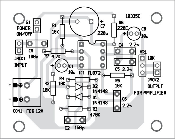
JACK1 and JACK2 may be fixed on the rear side, and switch S1 and VR1 can be mounted on the front side of the box.
DOWNLOAD PCB and Component Layouts: click here
Joy Mukherji is an electronics hobbyist and a small business owner in New York, USA, and Lucknow, India. His interests include designing radio-frequency circuits

super
Thanks for the feedback!
Hello. In the tranceivers already have built noise reduction like dnr dnf dbf .
Can this circuit improve more? Somebady tray?