
 Staircase signals find many applications in the field of electronics, such as in television systems, telemetry, and analogue and digital communications. Here is a circuit illustrating the basic principles of staircase waveform generator. Advantages of this circuit are: simple, low-cost, no complex programming, easy-to-assemble on a breadboard and adjustable staircase waveform outputs of variable step sizes and durations.
Circuit and working
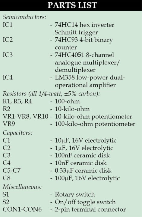
The circuit diagram of a simple adjustable staircase waveform generator is shown in Fig. 1.
IC1 (74HC14) is a hex inverter Schmitt trigger that generates oscillatory pulse (square wave) and gives an output clock at pin 14 of IC2 (74HC93), which is a 4-bit binary ripple counter. Pins 8, 9 and 12 of IC2 are connected to select pins of IC3 (74HC4051), which is an 8-channel analogue multiplexer/demultiplexer with three digital selected pins 9, 10 and 11. Input pins of IC3 are connected to eight potentiometers of 10-kilo-ohm each.
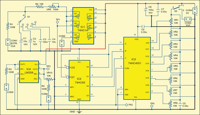
Variable step sizes are obtained by varying these potentiometers. Depending on the selected pins and values of potentiometers, we get different types of staircase waveforms at output pin 3 of IC3. When these waveforms are further given to the input pins of IC4 (dual op-amp), it simply buffers them. Fig. 2 shows four different types of staircase output waveforms obtained at CON5.
Vcc depends on the ICs used in the circuit and can be 5V. With CMOS ICs like 74Cxxx and CD4000B, we can use Vcc up to 15V.

Construction and testing
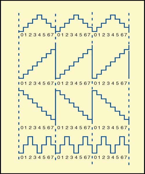
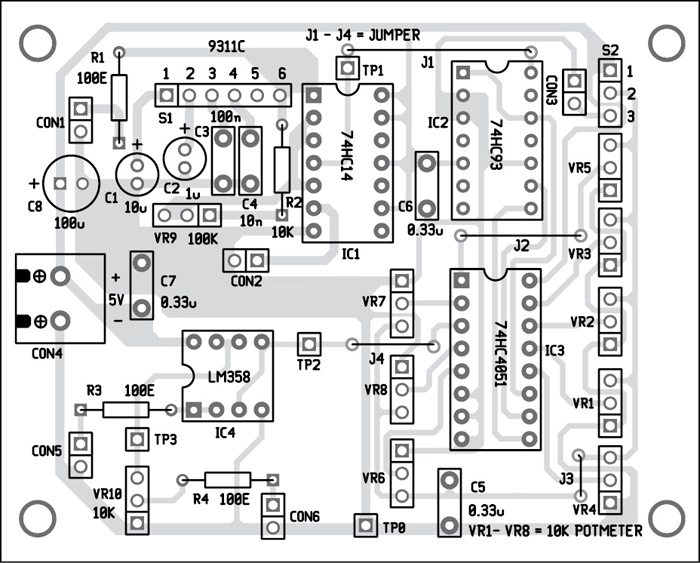
An actual-size, single-side PCB layout of the simple adjustable staircase waveform generator is shown in Fig. 3 and its component layout in Fig. 4.
The frequency at pins 1 and 2 of IC1 depends on the type of IC used and values of capacitors and resistors connected to gate N1 of the IC. It can be from 1Hz to 1MHz. If you use an external frequency, move S1 to position 5 to bypass capacitors C1 through C4.
Switch S2 selects the source of reference voltage for VR1 through VR8. In the first position (1), Vcc is used as reference source. In the second position (3), signal from connector CON3 is used as reference source.

 The fixed-amplitude staircase output waveform is obtained at CON5 and variable-amplitude staircase waveform is obtained at CON6.
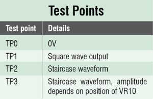
Each waveform consists of eight clock pulses, zero through seven. The height of each step is adjusted according to the need using potentiometers VR1 through VR8. The frequency of the step is determined by the oscillator around gate N1 of IC1 or by the external clock signal applied to connector CON1. For troubleshooting, check the various test points and ensure you get the outputs as per table.
Download PCB and Component Layout PDFs: click here
The author was a researcher and assistant professor at Technical University of Sofia, Bulgaria, and expert-lecturer at OFPPT, Casablanca, Kingdom of Morocco. He is currently working as an electronics engineer in the private sector in Bulgaria

i am confused with the rotary switch, about its connection , and which switch should be used,,,,send me the particular name of switch