


The high impedance audio buffer circuit described here can be used to enhance the AC input impedance of audio amplifiers that are used with pickups in musical instruments.
Some signal sources for preamplifiers, passive pickups for electric guitars or sensors based on capacitors require very high-impedance of over 5-mega-ohm. This can be achieved easily with junction field effect transistor (JFET) but may require special design of the printed circuit board (PCB), appropriate construction techniques of the box, proper cables and connectors.
This circuit provides a solution for a high-impedance, low-cost, low-quiescent current, buffer-follower based on PN4393 JFET.

High impedance audio buffer circuit
The circuit of the high impedance audio buffer with JFET is shown in Fig. 1. It has almost unity gain and relatively-low-output impedance. The buffer can be used with any appropriate JFET including J201, J202, J113, PN4391, PN4392, PN4393, 2N5457, 2N5458, 2N3819, BF245B, MPF102 or similar. Although there are some differences between these JFETs, all of these can do the job depending on the input signal range. However, care must be taken because some JFETs are not pin-to-pin compatible.
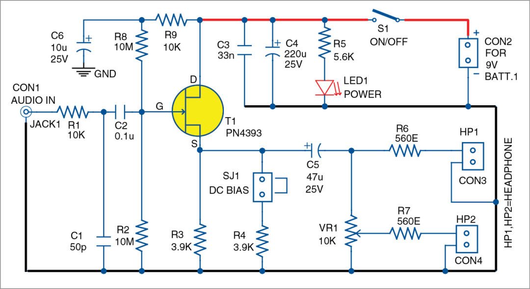
Audio input is applied to connector CON1. Input impedance depends mainly on the values of resistors R2 and R8 and is around 5-mega-ohm. If resistors R8 and R9 and capacitor C6 are omitted, input resistance will depend mainly on R2 and will be around 10-mega-ohm.
Value of R2 can be increased but it may be difficult to maintain the high input resistance during the practical usage of the circuit. Resistor R1 and capacitor C1 are used for protection and filtering functions for the input of the buffer, respectively. C1 can be omitted but not R1. Values of R1 and C1 can be changed as per requirement. Capacitor C2 is used to remove DC input components.
 Resistors R8 and R9 between gate G and drain D of transistor T1 are not always needed. So resistor R8 is not necessarily equal to R2. Also, R8 will reduce the input impedance. Use of high-value resistors R2 and R8 may increase input noise, so care must be taken while selecting their values.
Resistor R9 and capacitor C6 are for filtering noise from the power source. These can be omitted if the power source is clean. But filtering capacitors C3 and C4 should not be omitted.
Resistors R3 and R4 provide DC bias for the JFET. Resistor R4 is connected to transistor T1 through shorting jumper SJ1. Range of R3 is from 1-kilo-ohm to 10-kilo-ohm. Lower values will provide lower output impedance but will increase the power consumption. Bias depends on the input signal, parameters of the JFET and power supply.
JFETs
JFETs have wide tolerances, which is the main issue during their application. Fortunately, this is not a problem here. If a single circuit is required, choose an appropriate value for R3 depending on the JFET. In that case, SJ1 and R4 can be omitted. If some other JFET devices are required, connect R4 to source S of the JFET through SJ1 without changing the value of R3 to adjust the circuit to the parameters of the JFET.
This buffer has two outputs available at connectors CON3 and CON4. The outputs can drive loads of 10-kilo-ohm or more, simultaneously. Higher impedance loads are preferred. The loads can be reduced to 2-kilo-ohm without overloading the circuit, but amplitude of the signal will drop. Usually, that is not a problem. The circuit can drive two high-impedance 2-kilo-ohm headphones (HP1 and HP2) connected to CON3 or CON4 (a total load of 4-kilo-ohm).
Signal level on output CON3 is not adjustable but signal level on CON4 is, using potmeter VR1.
Choice of power supply depends on the peak-to-peak amplitude from the signal source. One or two 9V batteries of type 6F22 can be used. These provide 9V or 18V of power supply voltage, covering practically all passive pickups for the musical instruments and other high-impedance sensors. Some JFETs allow higher power supply. A well-filtered DC wall adaptor can also be used.
Construction and testing
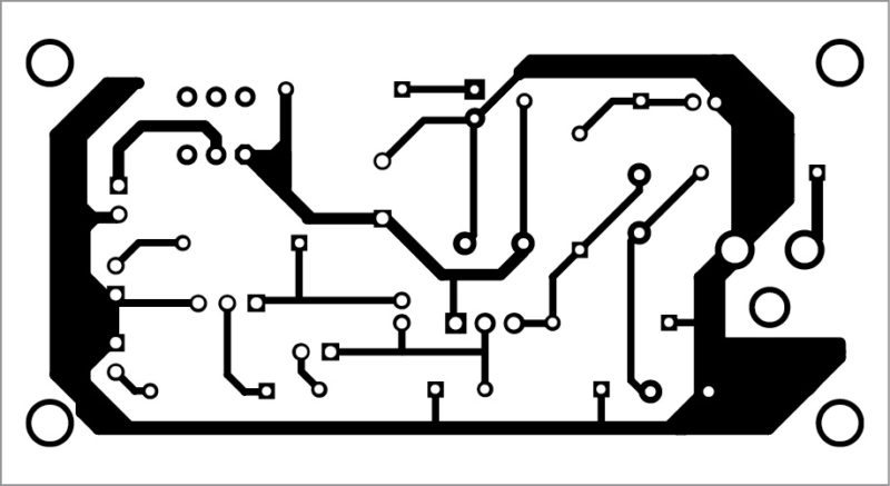
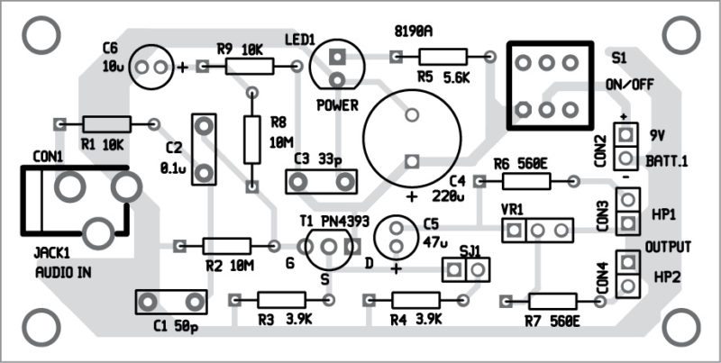
A single side PCB for the high impedance audio buffer with JFET is shown in Fig. 2 and its component layout in Fig. 3.
This circuit may require appropriate selection of values of resistors R3 and R4 in order to optimise the peak-to-peak amplitude of the output signal. It is appropriate for battery operation, which is important for portable applications.
The circuit can be mounted in a small box near the pickup or attached to the strap of the string instrument. Due to its high input impedance, input cable should be shorter than one metre and shielded or, at least, twisted. The gain is lower than unity but that is not a problem because most pickups provide strong signals.

can I know more about this circuit please..
thank you..
Please elaborate your query.
What is the output power ..???
Is that power can used to drive a large speakers??
an u say what is the aadvantages and future use of this project
Hello sir the output power is very less how to improve that, and i have an doubt that is this circuit is used to drive an 8ohm speaker or not?