


In our fast-paced digital world, staying connected is essential, and a reliable power bank is a must-have accessory for smartphone users.
This smartphone power bank project utilizes two key integrated modules along with a lithium-ion battery to deliver efficient charging on the go.
The first module serves as a lithium-ion battery charger, ensuring safe and quick charging, while the second is a DC-DC boost converter, stepping up the voltage to provide the standard 5V output for USB devices.

In this guide, we’ll dive into the details of this innovative power bank project, providing you with all the information you need to create your own portable charging solution!
Power Bank Circuit and Operation
The circuit diagram of the power bank is shown in Fig. 1. It consists of a USB lithium-ion charger module (USB-IN), 3.7V/2600mAh lithium-ion battery (BATT.1), on/off switch (S1) and DC-DC boost converter module (USB-OUT).
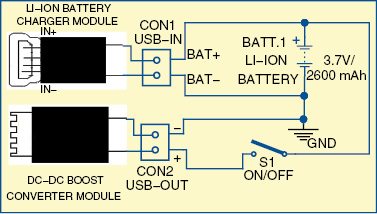
Here, a lithium-ion charger module based on TP4056 IC, rechargeable lithium-ion battery (Samsung type 18650) and DC-DC converter module based on pulse frequency modulation (PFM) technology are used.
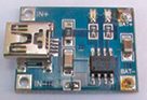
The battery charger module, shown in Fig. 2, is designed around a dedicated lithium-ion battery charger TP4056 chip and populated with SMD components. This onboard charge controller chip handles BATT.1 charging operation by processing the 5V DC input supply received through the USB socket (or through IN+ and IN- terminals).
Output terminals (BAT+ and BAT-) can be directly connected to BATT.1. Two onboard SMD LEDs located on top of the circuit board provide charging status indications.
BATT.1 is used as the power reservoir. Since only a 3.7V DC supply is available from BATT.1, DC-DC boost converter is used to cater to the stable 5V DC supply at output. If an input voltage of 0.9V to 5V DC is available, this converter gives stable 5V DC output through its USB socket, with a conversion efficiency up to 96 per cent.
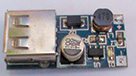
The DC-DC boost converter module, shown in Fig. 3, is an SMD module with a PFM chip at its heart. Input DC supply fed through input terminals (+ and -) is processed by this dedicated chip to give a stable USB standard DC supply via the standard USB socket at its output.
An onboard SMD LED, fitted near the input terminals, works as a power-status indicator. Switch S1 is included to route DC supply from BATT.1 to the converter.
Also check: Batteryless power bank project.
Operation Application
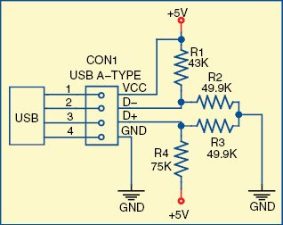
Almost all smartphones look for signals/levels on D+ and D- of the USB interface that indicate the charger’s current capability. A full-speed device will use a pull-up resistor attached to D+, as shown in Fig. 4, to satisfy itself as a full-speed device. The pull-up resistor at the device end will also be used by the host or hub to detect the presence of a device connected to its port. Without this resistor logic, the USB assumes there is nothing connected to the bus.
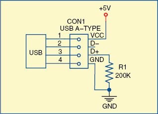
In case of a charging error, pull down D+ line of the USB output socket (in converter module) with the help of a 200-kilo-ohm resistor as shown in Fig. 5.
Construction and Testing
Assemble all components of the power bank circuit as per Fig. 1.
Follow the testing operation given below:
1. Connect the charger module to CON1 (USB-IN) either through an AC adaptor or provide a 5V DC supply through a PC or laptop using a USB cable for charging BATT.1.
2. Connect BATT.1 across CON1 for charging. A red-coloured LED will turn on, showing the charging status of BATT.1. When the battery is fully charged, a blue-coloured LED will turn on. You may remove the charger connected at USB-IN.
3. You can now charge your smartphone by connecting it to the USB socket of the converter module (USB-OUT) using a USB cable and closing switch S1. A red-coloured LED of the converter module will turn on, showing the charging status of the smartphone.
EFY note: Connect the terminals of BATT.1 to USB-IN and USB-OUT with the correct polarity.
Future Enhancements
- Fast Charging: Incorporate quick charge technology to reduce charging time for connected devices.
- Wireless Charging Capability: Add wireless charging features to accommodate newer smartphones.
- Solar Charging Option: Integrate solar panels to allow charging of the power bank using solar energy.
- Smart Features: Implement a microcontroller to add features such as battery level monitoring via an app or display.
Conclusion
The Power Bank for Smartphones project not only provides a practical solution to the common problem of battery life but also offers a hands-on learning experience in electronics and power management.
By understanding the principles behind charging circuits and power storage, this project paves the way for further exploration of renewable energy and portable electronics.
As mobile technology continues to evolve, enhancing power banks with new features will ensure they remain relevant and useful in our increasingly mobile world.
Check other Mobile Charger Projects
Mobile Cell Phone Charger Circuit using 555 Timer
T.K. Hareendran is an electronics hobbyist, freelance technical writer and circuit designer.
To read other exciting Electronics Projects: click here
This article was first published on 12 December 2016 and was recently updated in 2025.

How to achieve all modules/components
I want all the components of this project, some documents and demo presentation
@Venugopal : Sorry, asked components aren’t available with us. More other project kits, visit kitsNspares.com
Is there any other way in which we can make the same powerbank otherthan readymade parts?
@ Venugoapl & @arvind contact me….. on 9665031822. I have solution for Power Bank.
Explain me simply sir and i need a video of making
Comment: hi sir,
well explained article. How can one get the complete circuit of this power bank. thanks sir.
I didn’t understand pull up and pull down resistor concept, please explain me.
I was searching for the diagram of the charger and converter module not for the connection diagram
Hi can someone tell me how to make a power bank with two output 1amps and 2amps with pass through charging?
I have on rechargeable battery of 4.5v with charging circuit of 230v. Is it possible to make power bank from it?
I need power bank DC to DC module, if any one is selling, contact me 8561908866
may i know where can i buy the components to make a DIY power bank?
May I also know, can the 3V t 5V converter be replaced with a step-up transformer?
Hope i can get good explanation on this matter.
I am also working on the same issue if any answer plz let me know
hi can u help me for making power bank 7.4v lithium batt
Electronics Projects: Power Bank for Smartphones
What would be the approximate cost of this project.
Is this circuit compatible with 20,000mah battery?
Please send mobile charger/power bank with all protection with ckt diagram cap. 2Amp for mobile charger o/p to get component easily
How many batteries can be. Connected
I can answer your questions. just email me at:[email protected]
Hi. I’ve built the powerbank in accordance with the given circuit. The smartphone that I’ve connected charges, however, it’s very faint; while it prevents the phone battery charge from dropping any further, it can’t manage to increase the charge of the battery. I’ve been testing the circuit for about 30 minutes now, and I’ve checked that the compound battery voltage has dropped to 1.4 V from 3.7 volts( I’m using four 18650 4300mAh batteries in parallel) . What can I do to improve the performance of the circuit?
The circuit is well connected and the batteries are fully charged.
while i connected the smart phone to the power bank…after about seven or eight seconds, the out put at the USB terminal drops to zero. But the batteries are showing full voltage.
any solution can be suggested please.
The circuit is well connected and the batteries are fully charged.
while i connected the smart phone to the power bank…after about seven or eight seconds, the out put at the USB terminal drops to zero. But the batteries are showing full voltage.
any solution can be suggested please.
The output drops to zero after few seconds whether the load is connected or not connected.
Do we need both Pull up and Pull down configuration or anyone ?
Comment:pls I am so interested how to repair powerbank but I have to understand d function of all d components.this is my no./Whatsapp +2348056676386 or +2348060593115 email [email protected]. you can send me links,vidio that can help.tanks