
(B) is the Bus-Connectivity area. It shows the interconnections between the different IP cores, memory and the processor. There are two types of buses, namely, the Processor Local Bus (PLB) and the local Memory Bus (LMB). The vertical line represents a bus and the horizontal line represents a bus interface to an IP core. A hollow connector represents a connection that you can make and a filled connector represents a connection made. To create or disable a connection, click the connector symbol.
(C) is the View-Buttons tab. There are two buttons here, using which you can change between Hierarchical view and the Flat view. Hierarchical view is the default view in the System Assembly View panel in which the information about the design is based on the IP core instances in the hardware platform and organised in an expandable or collapsible tree structure. When you click the directory structure icon, the parts are displayed either hierarchically or in a flattened view.
(D) is the Console Window area. It displays all the textual information, warnings and errors that occur as the changes are made to the project, netlists and bitstreams, etc.
(E) is the System Assembly View in which you can view the project’s IP cores and the properties. It displays all hardware platform IP instances using an expandable tree and table format. The IP elements, their ports, properties and parameters, which are configurable in the System Assembly View, are written directly to the MHS file. There are three tabs in the System Assembly View, namely, the Bus Interfaces, Ports and the Addresses. The bus interface tab shows the following information for each core:
(i) Instance name (name of the core used to reference the core in the UCF)
(ii) Bus name (the bus to which the core is connected)
(iii) IP type (name of the IP core as in the IP catalogue)
(iv) IP version (the version of the IP core)

The Ports tab shows the user accessible ports of the IP cores and the nets to which they connect. The Addresses tab shows how the IP cores are mapped to the PLBs in the design
(F) is the Filters Pane area. It allows you to filter what is shown in the System Assembly View for simplified view of the design or in the case of many IP cores in the design.
16. Since we are using custom board for designing, the UCF file needs to be updated. Allot the FPGA pins to the LEDs, Clock and RST signals. The UCF file created for the ML501 board is shown in Fig. 12.

17. The download.cmd file is changed, as shown in Fig. 13, as the FPGA is the 4th device in the JTAG chain used. (The number assigned depends upon the JTAG being used.) Save the project
18. From the XPS menu, select Project → Export Hardware Design to SDK
19. In the dialogue box that appears (Fig. 14), make sure that Include Bitstream and BMM File are ticked and click Export Only
20. The bitstream will be generated and the project will be exported to SDK subsequently. Once it is done, we can progress to the next step
21. Open SDK by selecting Start → Programs → Xilinx ISE Design Suite 13.4_1 → EDK → Xilinx Software Development Kit
22. The first thing that the designer has to do is to enter the SDK workspace. SDK workspace is a folder wherein the software application(s) for a particular EDK hardware design are managed. The folder specified is shown in Fig. 15. You can choose any folder but it is better if the software folder is created inside the main project folder for ease of use
23. SDK opens with a Welcome screen. Select File → New → Xilinx C Project. Next, you have to specify the hardware platform. Click Specify on the window that appears. In the dialogue box that appears, type the name of the project as edk and use the Browse button under the Target Hardware Specification (refer Fig. 16) heading to navigate to C:\edk\SDK\SDK_Export\hw\system.xml file. Click Finish
24. The wizard that follows allows you to create a template software application for the project. The default is ‘Hello World’ example. We want to create a blank application. Select Empty Application and click Next, as shown in Fig. 17. Click Finish
25. An SDK window appears as shown in Fig. 18
26. In the Project Explorer, open the tree empty_application_0 → src. There is no source file in the folder. We need to add the source file. Select src folder and go to File → New → Source File. In the dialogue box that opens, specify the name of the source file to be created and the folder in which to put it, as shown in Fig. 19. Click Finish. If you now expand the src folder, you will find led.c inside that folder
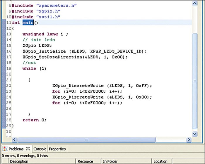
27. Click on led.c and paste the code given below onto it. Save the file. When you save the file, it is automatically compiled. You should get zero errors, as shown in Fig. 20
Download Source Code: click here
The C code first initialises the LEDs port and then sets the port as output port. Then the LEDs are switched on and off using a delay created by the ‘for’ loop
[stextbox id=”grey”]#include “xparameters.h”
#include “xgpio.h”
#include “xutil.h”
//===========Program===========//
int main () {
unsigned long i;
//Init LEDS
XGpio LEDS;
XGpio_Initialize(&LEDS, XPAR_LEDS_
DEVICE_ID);
XGpio_SetDataDirection(&LEDS, 1,
0x00);
//Out
while (1)
{
XGpio_DiscreteWrite(&LEDS, 1,
0xFF);
for (i=0; i<0xF0000; i++);
XGpio_DiscreteWrite(&LEDS, 1,
0x00);
for (i=0; i<0xF0000; i++);
}
return 0;
}[/stextbox]
Select Xilinx Tools → Program FPGA. The bitstream gets loaded to the FPGA. The LEDs start blinking. If they do not blink, press the reset switch used in the design. On pressing the reset switch they will start blinking.
Conclusion
With this part, the series of articles on Designing with FPGAs is concluded. The articles were written with an aim to provide the electronics engineers, professionals and hobbyists an insight into different aspects of system design using FPGAs.
Varsha Agrawal is a scientist at Laser Science and Technology Center (LASTEC), a premier DRDO lab working in the field of laser-based defence systems. She has more than 13 years of R&D experience in the design and development of a variety of systems for defence-related applications. She has authored two books and published more than 20 research papers and technical articles


