
The 28nm family also provides a wider variety of metal options to support a broad range of product applications for better trade-off between performance and density. It only requires six metal layers instead of the traditional ten or more in conventional mesh FPGAs, and offers 1.8 times higher logic density, thanks to optimised interconnect.
TSMC offers three processes at 28nm. These are 28LP, 28HP and 28HPL processes. Millions of production wafers have come out of TSMC’s 28nm processes. In TSMC, 28HPM/C fast control logic can run at 525MHz or more, and pipelined FIRs can run at 450MS/s or faster.
Designers can improve SoC performance by using global slow and fast (SSG, FFG) signoff corners. These are enabled by TSMC’s tighter process controls with 28HPC/HPC plus over 28LP/HP/HPL/HPM. Improved performance enables the use of lower-drive (smaller) logic cells to close critical-timing paths.

28LP process. 28LP process has 20 per cent speed improved over 40LP process at the same leakage/gate.
28HP process. 28HP process targets CPU, GPU, FPGA, PC, networking and consumer electronics applications. It supports 45 per cent speed improvement over 40G process at the same leakage/gate. With higher performance coverage, 28HPM is ideal for many applications in networking and high-end smartphone/mobile consumer products.
28HPL process and 28HPM. 28HPL process reduces both standby and operation power by more than 40 per cent. Compared with TSMC’s 28LP, 28HPC provides ten per cent smaller die size and more than 30 per cent power reduction at all levels of speed. A comprehensive 28HPC IP ecosystem is also built and compatible with 28HPM, accelerating time-to-market for customers. 28HPC is also ideal for many applications in mid- and mid-to-low end smartphones, tablets and mobile consumer products.
EFLX cores
EFLX core is memory type and needs to be TSMC 28HPC-compatible. TSMC provides high-performance compact mobile computing, the most energy-efficient and high-performance method of manufacturing for customers looking to tap chip area and power saving benefits of mid- to low-end SoC designs.
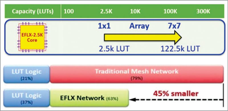
Architecturally, core tiles can be combined into arrays. For EFLX-2.5K, up to a 7 x 7 array is feasible for a total of 122.5k LUTs. This reminds of systolic arrays with multiple FPGAs of yesteryear, minus the nasty external chip-to-chip interconnect problems. EFLX tile array can implement an optimised data flow DSP pipeline, or multiple EFLX tiles could be scattered across functional blocks in an SoC.
EFLX cores are RAM based, which is programmed from RTL and is converted into a stream of configuration bits. Current technology is EFLX-2.5K core, available in TSMC 28nm HPM/C and packing 2.5k LUTs, as the name implies.
EFLX cores consist of individual 2500-LUT (lookup table) cores. These add less than 15 cents to the total manufacturing cost of a device. These cores can be integrated into multiple circuit blocks in the same design, or tiled together to create arrays of 7 x 7 or more EFLX cores for better performance.
EFLX cores come in two sizes, and each of those can be tiled together to make larger arrays of the FPGA fabric. EFLX logic core incorporates 40 multipliers-accumulators (MACs) with 22-bit inputs and 48-bit accumulation. The MACs can be combined for double the precision and pipelined for high throughput. These can also be used as complex-number MACs for certain DSP algorithms. With the same number of LUTs, EFLX is 1.8 times smaller in total area than the traditional mesh of FPGA.
Each EFLX core is divided into reconfigurable building blocks (RBBs), tuned for existing synthesis tools. This allows highly-optimised interconnect and logic placement. Any RBB can connect with another RBB, on the same EFLX tile or another tile in a connected EFLX array, up to a practical limit of 7 x 7 array size. With a single EFLX core, it is possible to implement valuable functions such as software-reconfigurable I/O pin-multiplexers and crossbars, reconfigurable fast control plane logic, reconfigurable multi-stage FIRs or the ability to change custom hardware accelerators post production.
Individual EFLX core tiles can be snapped together to form M x N arrays using the same EFLX network for interconnect, making the power of the concept clear. In addition to local memory, many applications also require DSP capability. Tiles with DSP emphasis or logic emphasis can be mixed and matched in an array for optimisation.
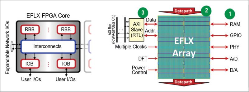
EFLX-100 core comprises three major blocks: RBBs of logic/DSP type, interconnect network and user I/Os. EFLX features full connectivity inside the core, and provides additional interconnects at the boundary to concatenate multiple cores via expandable network I/Os. Each core has an internal power grid (VDDH and VSS), which can be connected to the customers’ digital SoC power grid.
The core has power-control pins for power on and power gating, and includes configuration bits that are configurable via AXI, JTAG or a custom serial interface. On each side of the core there are two input clocks and two output clocks, which concatenate in EFLX arrays. Every LUT has an optional flip-flop at the output.
Additional logic implements carry chains for adders and comparators. Reconfigurable logic is interconnected by a reconfigurable interconnect, which allows any logic block to connect to any other. It also has patented interconnect that doubles density and only requires six or less routing layers for volume-chip compatibility.
EFLX-100 core is available in five different configurations and two nominal voltages, each optimised for different performance-to-power requirements for different target applications. Use of commercial synthesis tool chains also enables use of their other features including synthesis constraints and FPGA debug tools. The tools just need to know which tiles are being used and what arrangement we need to put these in (1×2, 2×2 and so on), let us say, to make up to 7 x 7 arrays of their 2500-LUT tile tailored for custom FPGA-in-a-chip.
EFLX-100 core is the ultimate in point-level reconfigurability where just a few gates are needed, and has targeted it for a mature TSMC 40nm LP/ULP process. Evaluation and prototyping of a single-core EFLX design gives customers the experience and insight to build flexibility into their RTL designs, even if the target application requires a larger EFLX array. EFLX cores available are TSMC 28HPM/C EFLX-2.5K core (either logic or DSP version) and TSMC 40ULP/LP EFLX-100 core (either logic or DSP version).
