

Modern broadband red and blue LEDs efficiently generate light that matches exactly with plants’ spectral requirements. LEDs are thus being increasingly used all over the world for indoor cultivation of a wide variety of plants. Experiments on LED-powered crop cultivation have also been carried out on the international space station.
The rising popularity of LED-based solid-state lighting systems is backed by cutting-edge research to support consumer expectations. A great deal of R&D on LED materials, processing techniques and device design is being carried out in academic, industrial and government laboratories around the world. Some of it is aimed at further improving the already impressive efficiency of these devices and bringing down their manufacturing cost while other work explores the quality of light generated by LEDs and ways of further prolonging their useful lifetime. Besides these, highly specialised LEDs for niche applications are also under development so that we will see their uses proliferate even more in the coming years.
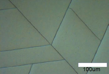
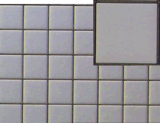
Perhaps most industrial R&D effort at this time is being directed at reducing the cost of production of blue-emitting gallium nitride LEDs. The main focus of attention is on replacing the sapphire substrate, on which gallium nitride LED device layers are grown, with silicon. If this can be done successfully then there will be great cost benefits to the LED industry. This is because sapphire substrates are significantly more expensive than silicon wafers and are also mostly available as only two inch diameter wafers. Much larger silicon wafers, with diameters as large as twelve inches, are commercially available at low cost, thanks to the silicon integrated circuit industry that uses such wafers for making a wide variety of analogue and digital chips. If gallium nitride can be grown on large diameter silicon wafers then each wafer will yield vastly more LED devices than the usual two inch diameter sapphire wafer. This is the principal driver for lowering the cost of LED chips. The main impediment in growing device-quality gallium nitride on silicon is the propensity for the gallium nitride layer to crack due to mismatch in the lattice parameter (distance between atoms) of gallium nitride and silicon (see figure 8 – left). Progress has been made in solving this problem by a variety of means such as growing gallium nitride on pre-patterned silicon wafers where the growth stress is accommodated in the ridges, leaving pristine gallium nitride in between (see figure 8 – right). There are several other benefits that result from changing the substrate from sapphire wafers to silicon wafers. Readily available equipment originally designed for processing silicon wafers can be used for fabricating LED wafers. In contrast to sapphire, the silicon base can be easily removed from gallium nitride-on-silicon wafers, freeing the actual LED structure which can then be placed on a metal substrate for much improved heat removal. This way much higher brightness LEDs can be easily produced. Several major LED manufacturers, such as Lumileds, Bridgelux and Lattice Power have active programmes in this area with expectations of large scale market introduction next year.

Other prominent research themes include work on zinc oxide – a promising alternative to gallium nitride for making blue LEDs. Making p-type zinc oxide is still a problem and thus research continues on new ways for doping zinc oxide to produce good p-type material. Several research groups are also working on the growth of ultra-narrow columns of gallium nitride called quantum wires that exhibit higher efficiency in light emission. Scientists from Osram, in particular, have reported significant advances in their quest for quantum wire LEDs. Yet other research collaborations have been exploring the incorporation of colour-converting cadmium selenide quantum dots with gallium nitride LEDs to produce narrow-band LEDs of high colour purity. Several research laboratories are also busy improving the structure of LED device layers in an effort to boost their efficiency by eliminating mechanisms that lead to non-radiative energy loss in LEDs.
With so much being staked on LEDs and the promise of many further developments in the near future, the prospects for solid-state lighting are brighter than ever before. Half a decade from now, LED bulbs and luminaires will be as commonplace as incandescent lamps are at the time of this writing. In another few years after that, traditional tungsten filament lamps will seem as quaint as vacuum tubes; completing the revolution to an era dominated by semiconductor-based light sources.
The author, Faiz Rahman, is a technology officer at Electrospell Ltd, UK.
