“Everything can be made in some way better—stronger, lighter, cheaper, easier to recycle—if it’s engineered and manufactured at the nanometre scale.”

—Stan Williams director-Quantum Science Research HP Labs
JULY 2011: The 21st century can easily be called the era of portable devices that are lighter, smaller and a whole lot powerful in configuration than their predecessors. All this has largely been rendered possible with the size of the processor shrinking to the nanometre scale. These small-sized processors, also called microprocessors, have enabled the electronics manufacturers to build products that are smaller in size, have faster processing speeds and are powerful. However, experts view this development more as the continuation of existing microelectronics rather than a breakthrough in the nanotechnology space. They believe that this is merely a small application of nanotechnology and doesn’t represent even an iota of the potential that nanotechnology holds for the future of electronics.
ndeed, nanotechnology is not merely about reducing the size of processors to nanometres. Its domain is vast and still remains largely unexplored. Considering the research happening across the globe, and the advances so far in this space in terms of the development of new circuit materials and so forth, the technology surely holds a lot of promise for the technologists and electronics industry alike.
Apart from this, nanotechnology is being also viewed as a solution to the limitations of the current technologies. If we look at the current situation of digital electronics, there is presently no credible alternative to silicon complimentary metal-oxide-semiconductor (CMOS); all other technologies having failed to meet the standards of logic circuits. The improvements in silicon technology are also getting closer and closer to the ‘brick wall’ and this worries a lot of technology professionals and industrialists. It is anticipated that sometime around the end of this decade (2018 or so), it will become physically impossible to etch smaller features in silicon. Another challenge is that at lesser than 20nm sizes, silicon becomes electrically ‘leaky,’ which can cause short-circuits.
Is ‘nano’ the way to go?
With the current materials and technologies nearing the upper limit, scientists and researchers have built a lot of hope around nanotechnology, which according to them can help in developing alternative methods and materials. They believe that someday nanotechnology will revolutionise the global economy by providing power tools that will produce high-tech products using low-tech resources at low costs.
There is no denying the fact that on the concept level, nanotechnology holds a lot of promise. But in spite of breakthroughs prophesied in this field by many a scientist and futurist, especially if we consider the application of nanotechnology in the field of electronics, there hasn’t been much headway ever since the technology’s emergence in 1990s. In fact, the term nanotechnology has become more of a misnomer with different groups defining its periphery and scope differently.
To demystify the term and gauge the direction towards which the technology is moving, we turned to a few technology experts.
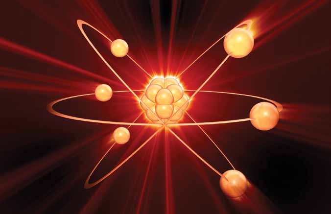
How much does ‘nano’ measure up in size?
Nanotechnology, which is sometimes shortened to ‘nano-tech,’ is the study of manipulating matter on an atomic and molecular scale. Generally, nanotechnology deals with structures sized between 1 to 100 nm in at least one dimension. It involves developing materials or devices possessing at least one dimension within that size. However, when it comes to the size, the opinions in the technology space are divided. There are some who claim that 45, 32 or 22nm technology does not qualify as nanoelectronics.
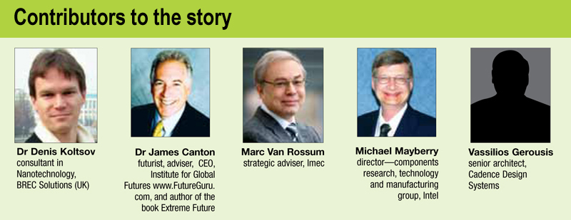
Vassilios Gerousis, senior architect, Cadence Design Systems, shares some of the varied viewpoints that are widely making rounds in the industry and amongst the science and engineering communities: “One opinion, which comes from the research fraternity deals with nodes that are between the dimensions of 10 nm and below, such as carbon tubes. Another opinion coming from the applied research domain caters to nodes between 14nm and 20nm. The third viewpoint is from the application side and is focused on 40nm and 28nm.”
Yet another view is that CMOS technology, even using nanoscale features, does not fully qualify as nanotechnology, because it uses mostly top-down fabrication to reach nanoscale dimensions. In this view, electronic devices should be labelled nanoelectronics only if these contain typical nanostructures such as carbon nanotubes or nanowires and dots. “However, the CMOS people themselves consider all technology nodes below 100 nm as nanoelectronics, since they comply with the basic definition of nanotechnology objects, i.e., structures with critical features below 100 nm,” says Marc Van Rossum, strategic adviser, Imec. “At Imec we share this view, and also consider several advanced top-down CMOS fabrication techniques such as extreme UV lithography and other nanoscale patterning tools to be part of nanotechnology,” he adds.