While lower in conductivity, PTF circuits have successfully served in a wide range of low-power applications at slightly higher voltages. Keyboards are a common application, but there is a wide range of potential uses for this cost-effective approach to flex circuit manufacture.
PTF technology consists of a simple set of basic building block materials, such as substrate, conductive inks, dielectrics, conductive adhesives and non-conductive adhesives/encapsulants. Underfills, required for flip chips, are commonly classified as packaging materials, but they are polymer-based systems that are a close kind of PTF.
Key capabilities of polymer thick-film flex circuits are:
1. Single-layer or double-layer screen through-hole circuitry
2. Low-cost, high-volume, roll-to-roll fabrication technology
3. Low-cost, screen-printed ink surface dielectrics
4. Economical choice for cost-sensitive applications

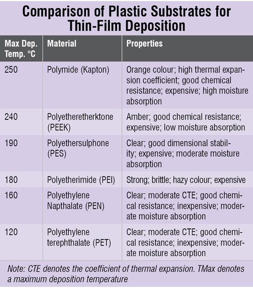
Integration process
Fabrication methods have an important effect on the characteristics, cost and stability. For example, instead of using a high-mobility material to achieve high device transconductance, it is possible to adjust the architecture. Employing short channel lengths is one way to achieve this. In conventional planar TFTs, the channel length is ultimately limited by the diffraction limit in the photolithography process. Vertical transistors, where the channel length is set by the thickness of the semiconductor, have been demonstrated to achieve submicrometer channel lengths, paving the way for high-transconductance devices using conventional materials such as a-Si.
Alternative approaches have also been developed to fabricate organic submicrometer TFTs uniformly over large areas. One such approach is based on a novel edge effect that is induced by spin-coating a polymer onto a prepatterned structure, as shown in Fig. 8. Polymer TFTs, with channel widths as narrow as 400nm, can be fabricated by this method.
One key advantage of this method is that, it facilitates the use of low-resolution patterning techniques, such as shadow masking, to create highly reproducible submicrometer features, thereby obviating more conventional, time-consuming lithographic processes. This, combined with inkjet printing, provides an exciting opportunity to apply on-demand material deposition and desktop-programmable wiring of ad hoc patterns. The latter has already been demonstrated for CNT and graphene-based inks.Though rather exotic, such innovative fabrication techniques will facilitate the technologies’ widespread usage for fabrication of TFT with high transconductance.
Any manufacturable device has following essential characteristics:
1. Superior and prespecified performance, with reproducibility, uniformity and reliability
2. High yield to acceptable tolerance
3. Simulations exist for both reverse engineering during development and right-first-time design
Some novel processes have been developed to fabricate solution-processable TFTs with one-step self-aligned dimensions in all functional layers. The TFT-channel, semiconducting materials and effective gate dimension were controlled by a one-step imprint process and subsequent pattern transfer, without the need for multiple patterning and mask alignment, as shown in Fig. 9. Both p- and n-type organic TFTs have been demonstrated using this method.
In the case of n-type TFTs, Li et al reported that 20 transistors were fabricated without process optimisation, with a yield of 100% and a variation in mobility and on/off current ratio of a factor of 3 and 5, respectively. All the used techniques (imprinting, wet/dry etching and inkjet printing) are already available in roll-to-roll processes. The demonstrated high-resolution features, mask-alignment-free process and compatibility to roll-to-roll fabrication show that these and similar techniques are commercially attractive, inexpensive and ready to use. It is expected that these methods can be extended to the level of integrated complementary metal–oxide–semiconductor (CMOS) circuit fabrication.
Part 2 of the article, in next issue, will cover some very interesting aspects of the application of flexible electronics in various sectors.
To be concluded next month
The author is a final year student of KMIT afflicted to JNTUH. This article is based on a paper he prepared for a technical seminar on flexible electronics