

Hardware Demonstration
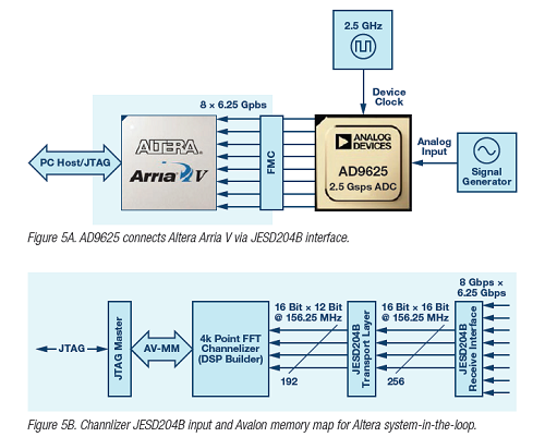
The project demonstrates the ADC interface and the channeliser function. A signal generator produces a sinusoidal tone as the ADC input. The ADC output is connected to the system-on-chip (SoC) development kit using the industry-standard FPGA mezzanine card (FMC) interface. The JESD204B standard defines data rates to logic devices in various lane configurations. The JESD204B interface in this demonstration is configured to use the 8-lane transceiver mode, as shown in Figure 5A and Figure 5B. The samples received over JESD204B interface are fed into the channeliser IP, which is configured to receive 16 samples concurrently using 16 input wires (Parameter M in Figure 4). Depending on the number of fast Fouriet transform (FFT) points, a full FFT frame is divided into multiple time slots. For example, a 1024-point FFT requires 1024/16 = 64 time slots to complete. Filter bank coefficients and FFT processing stages switch automatically according to the time slot. Channeliser IP was developed using tools like DSP builder advanced (DSPBA), a model-based design flow tool from Altera that enables design, evaluation, and verification of algorithms in MATLAB/Simulink environment. Once the algorithm is optimal, DSPBA generates a code that can be deployed on FPGAs.

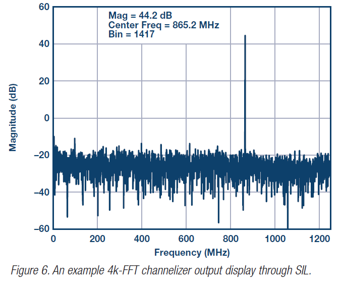
The channeliser output is stored in on-chip memory and is verified through system-in-the-loop (SIL) tool, which uses a MATLAB API to trigger on-chip registers to start logging for data visualisation. Once triggered, a single iteration of FFT processing is executed and the resultant data is stored into on-chip static random-access memory (SRAM). The MATLAB API extracts data through the memory map from SRAM to a MATLAB host. Once uploaded to MATLAB, the samples are plotted on the screen.
The channeliser can switch to different FFT size easily through a MATLAB setup script. Such flexibility ensures a future upgrade path and potential design reuse across different system configurations. As an example, Figure 6 shows a 4096-point FFT output from the SIL.
Faster EW solutions
Next-generation high speed converters offer solutions to provide higher instantaneous bandwidth without compromises on system sensitivity, and provide more flexibility in frequency planning or relieve a mix downstage on the front-end RF strip. However, achieving bandwidth data analysis in the 1GHz range can pose challenges to designing a high performance system.
To solve this problem, channelisers can be used to analyse these wide bandwidths while maintaining high performance. The GSPS RF ADCs coupled with configurable channeliser IP cores provide next-generation system designers a faster solution to the ever changing electronic warfare environment.
Rob Reeder is a senior system applications engineer in the Aerospace and Defence Applications Group, and Duncan Bosworth is the director of marketing and applications in the Aerospace and Defence Business Unit at Analog Devices Inc. Ronak Shah is the system engineer and manager, and Dan Pritsker is a senior system design engineer at Altera Corporation.


