 Nowadays, LED message displays are becoming very popular for transmitting information to large groups of people quickly. These can be used indoors or outdoors, in places such as railway platforms, public transport systems, traffic signals, highway signboards, banks, public offices, hotels, training institutes, nightclubs and shops. Compared to LEDs, liquid-crystal displays (LCDs) are easy to interface with a microcontroller for displaying information as these have many built-in functions, but these can’t be observed from a distance, and large-size LCDs are very costly.
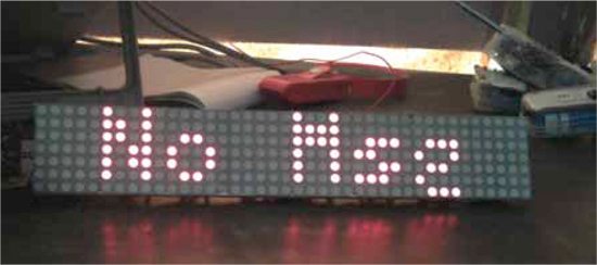
Presented here is a GSM-based, eight-digit dot matrix display that can show an eight-digit message sent via any mobile phone, from any place around the world, to the mobile number of the SIM in the GSM module of the display. Size of the display is 7×40, which is made using 5×7 dot-matrix LED modules.
Circuit and working
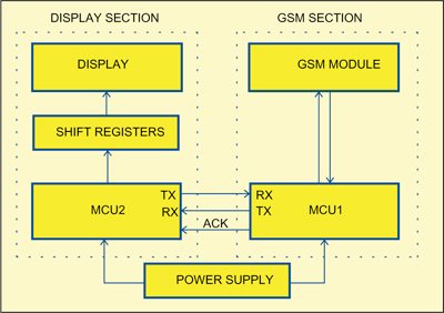
Fig. 2 shows the block diagram for GSM-based moving message display. For simplicity, the complete circuit is implemented into two parts: GSM section and display section.
GSM section. The GSM section comprises a GSM module with a dedicated SIM card inserted and a microcontrolle unit (MCU1). When a new message is received, MCU1 receives the corresponding frame from the GSM module. MCU1 then processes the data received and extracts the message from the complete frame. Once a new message is extracted, the GSM section informs the display section and sends the message via serial interface.
Display section. This section comprises a 7×40 dot-matrix display and a microcontroller unit (MCU2). MCU2 receives the message from MCU1 on serial interface. This message is stored in an array. The message is processed and corresponding serial data are sent to the LED drivers (shift registers) that are connected in the daisy chain.
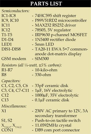
Fig. 3 shows the circuit of GSMbased dot-matrix display. It comprises two P89V51RD2 microcontrollers (IC9 and IC10), regulator 78S05 (IC12), shift registers (IC1 through IC8), MAX232 driver (IC11), MOSFETs (T1 through T5), 5×7 dot matrix modules (DIS1 through DIS8), GSM module SIM300 and a few discrete components.
The 230V AC mains is stepped down by transformer X1 to deliver a secondary output of 12V, 3A. The transformer output is rectified by a full-wave rectifier comprising diodes D1 through D4, filtered by capacitor C12 and regulated by IC12. Capacitor C13 bypasses the ripples present in the regulated supply. The generated 5V is supplied to the complete circuit. LED1 acts as the power indicator and R8 limits the current through LED1.
The microcontroller used in the GSM and display sections is P89V51RD2, which is an 8-bit microcontroller with 64kB Flash and 1024 bytes of data RAM. The P89V51RD2 has three 16-bit timers/counters, programmable watchdog timer, eight interrupt sources with four priority levels, serial peripheral interface (SPI) and enhanced UART, programmable counter array with PWM and capture/compare functions, and four 8-bit input/ output ports (of which three are high current). It also has an on-chip oscillator and clock circuitry, which operates up to 40MHz crystal. It supports 12 clocks per machine cycle (default) and 6 clocks per machine cycle modes, which are selectable via software. The Flash program memory supports both parallel programming and serial insystem programming (ISP).
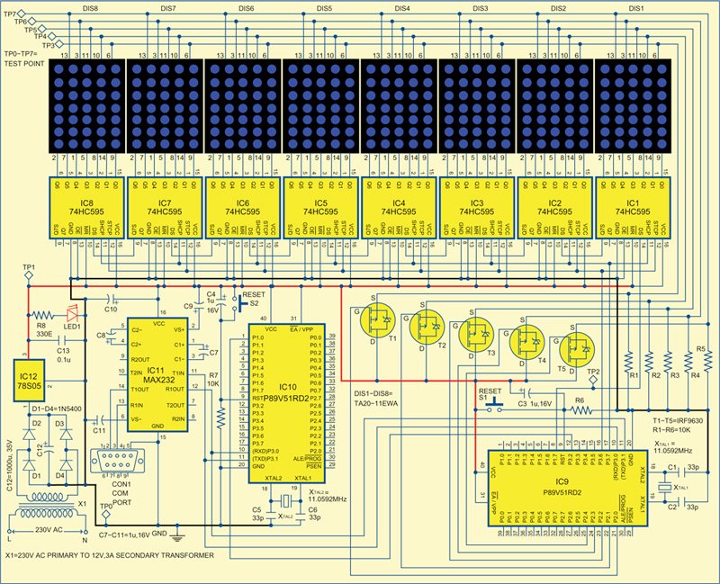
Microcontroller IC10 is interfaced to the GSM module using MAX232 driver. The GSM module is a specialised type of modem that accepts a SIM card and operates on the subscriber’s mobile number over a network, just like a cellular phone. Basically, SIM300 is a triband GSM/GPRS engine that works on EGSM 900MHz, DCS 1800MHz and PCS 1900MHz frequencies. GSM modem is RS232-logic-level compatible. Here MAX232 is used to convert TTL into RS232 logic level and vice versa.
Combination of resistor R7 and capacitor C4 provides the power-on reset for microcontroller IC10. Switch S2 is used for manual reset. An 11.0592MHz crystal (XTAL2) along with two 33pF capacitors provides the basic clock frequency. Microcontroller IC10 receives a frame corresponding to every new valid message received by the GSM module. This frame is further processed and the message extracted out of it. Thereafter, an acknowledgment is sent through port pin 1.0 to the display section indicating that a new message will be transmitted.
Microcontroller IC9 receives this signal and immediately jumps to the receive module in the program and the message data is serially received. TXD and RXD lines of IC9 are connected to RXD and TXD pins of IC10.
Download PCB and Component Layout PDFs: Click Here
Download Source Code: Click Here
Microcontroller IC9 controls the display unit. Once the complete message is received, it processes the data and serially sends it to the shift registers to drive the rows. The shift registers have a serial input (DS) that receives the message data through port pin P1.7 of IC9.
The data in each register is transferred to the storage register on a positive-going transition of the STCP input received from port pin P3.6 of the microcontroller IC9. Data is shifted on the positive-going transitions of the SHCP input received from port pin P3.7. Serial data output Q7S is used for cascading. Output enable (OE) pin is connected to ground for data in the storage register to appear at the output automatically. Microcontroller port pins P2.0 through P2.4 are connected to gates of MOSFETs T1 through T5 to drive columns C1 through C5 of all the dot-matrix display modules.
Resistor R6 and capacitor C3 provide the power-on reset to IC9. Switch S1 is used for manual reset. An 11.0592MHz (XTAL1) crystal along with two 33pF capacitors provides the basic clock frequency to microcontroller IC9.
Working of the system is straightforward. When you power-on the system after complete set-up, “No Msg.” is displayed intimating that the system is waiting for a new message. Write an eight-character SMS with a ‘#’ (which is the ninth character) at the end to indicate completion of the message. Send the message to the mobile number of the SIM in the GSM module. The same message will be shown immediately on the display.
Construction and testing
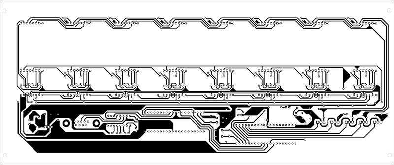
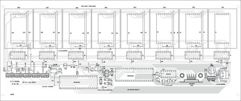
PCB layout for the moving-message display is shown in Fig. 4 and its component layout in Fig. 5. Please note that both these figures are scaled down to fit in the page. Assemble the circuit on a PCB as it saves time and minimises assembly errors. Carefully assemble the components and double-check for any overlooked error. Use IC bases for ICs. Before inserting the ICs, check the supply voltage.
First, insert the SIM in the GSM module and power it ‘on.’ Red and green LEDs of the GSM module indicate power-on and signal reception, respectively. The GSM module is connected to the circuit through CON1. Make a call on the SIM number in the module. A ring will be heard if the call gets connected successfully. Now, send the message through your mobile. It will immediately appear on the display.
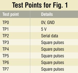
Check the correct power supply at TP1 with respect to TP0. You can observe the scanning at TP3 through TP7 using an oscilloscope. The serial data for shift resistors can be observed at TP2.
Software
The source program for the microcontrollers is written in ‘C’ language and compiled using Keil μVision4 compiler. The generated hex code is burnt into the microcontrollers by using a suitable programmer.
GSM section. The commands used to configure the GSM module are:
1. AT+CRES. This command is used to reset the GSM module.
2. AT+CMGF=1. This command is used for setting up the GSM module to send data in ASCII format.
3. AT+CNMI=2,2,0,0,0. This command is used to get complete message on the serial port.
Functions used in the program of the GSM section are:
1. receive( ). Receives serial data from the GSM module and saves it to a predefined location
2. msdelay( ). Provides delay
3. Transmit_data( ). Sends serial data to the display section
4. Gsmcmdsend( ). Sends GSM commands to the GSM module
Display section. Functions used in the program of the display section:
1. datazero( ). Clears the data array
2. clock1( ). Provides clock for serial shift register
3. datalatch( ). Provides latch signal for shift register
4. msdelay( ). Provides delay
5. datash( ). Shifts data in the shift register
6. receive( ). Receives serial data from the GSM section
7. default_msg( ). Displays default message “NO Msg”
8. data_compare( ). Compares the data with character set
9. data_insert( ). Inserts serial data
10. dot_display( ). Displays the message


I want this kit …. gsm based dot matrix display …
Kit isn’t available for this project. But you may visit kitsNspares.com where you can get wide range of DIY projects with all required components and PCB.
why mosfets are used???
nice project tnx…
You are most welcome.
Please can I get a detailed explanation of how the circuit works and the code? Thank you
I will love to build this project. please can I get a detailed explanation and the code? thanks
Thank you for posting this project. Please I will like to build this. Can I get the code?
Excuse I need proteus simulation for this project
What changes do i need to make if i want 15-18 characters?
can i use AT89S51 instead of P89V51RD2?