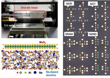
Researchers at Yonsei University and Sungkyunkwan University have developed a solution processing method to fabricate wafer-scale transistor arrays using molybdenum-disulfide.

Engineers have been trying to develop more efficient and cost-effective approaches for mass-producing electronic components and devices. In recent studies, researchers have explored the possibilities of creating electronics using solution processing techniques, which involve depositing materials with electrical properties onto a surface from a solution.
Researchers at Yonsei University and Sungkyunkwan University in South Korea have developed a solution processing method to fabricate wafer-scale transistor arrays using molybdenum-disulfide, an inorganic compound. Previously, the researchers showcased wafer-scale electronics utilizing different solution-processed 2D materials. Expanding on this research, the latest study aimed to optimize electronic properties while ensuring scalability.
The team employed a commercial slot-die printing process to fabricate their wafer-scale transistors. This method involves depositing liquid materials onto various substrates, including glass, metals, or polymers. The scientists formulated inks comprising nanosheets of molybdenum disulfide and sodium-embedded alumina. Subsequently, they utilized slot-die printing to apply these inks onto a substrate, forming semiconducting and gate dielectric layers. For achieving significant scalability, a slot-die coater, an industrial-level coating method, was employed to uniformly cover solution-processed dielectric and semiconducting channel layers on a 5-inch wafer. The team utilized a distinctive dielectric layer known as sodium-doped alumina to showcase high-performance electronics, enabling the highest field-effect mobility up to 100 cm2/Vs using solution-processed MoS2 thin films.
During the preliminary assessments, the transistors developed by the researchers showcased impressive performance characteristics. They displayed average charge carrier mobilities of 80.0 cm² V⁻¹ s⁻¹ in field-effect transistor measurements and 132.9 cm² V⁻¹ s⁻¹ in Hall measurements at room temperature. To further exemplify the capabilities of their transistors, the team utilized them to create various devices, such as NOT, NOR, NAND, and static random-access memory.
The researchers believe that the most significant contribution of this work is introducing a fresh avenue for high-performance, large-scale 2D material-based electronics through an industrial-level coating technique. In future, the researchers aim to focus on broadening the range of solution-processed material candidates, encompassing various electronic properties like electronic type and bandgap.
Reference: Yonghyun Albert Kwon et al, Wafer-scale transistor arrays fabricated using slot-die printing of molybdenum disulfide and sodium-embedded alumina, Nature Electronics (2023). DOI: 10.1038/s41928-023-00971-7


