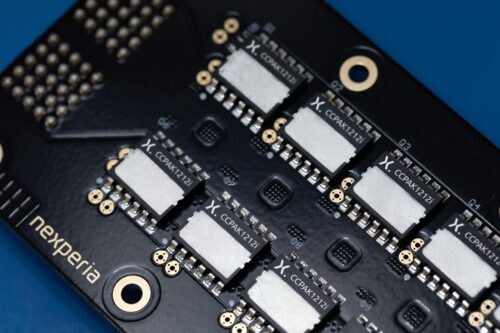
Merging the advantages of copper-clip packaging with wide bandgap semiconductors.

Nexperia has unveiled its latest innovation, Gallium nitride (GaN) field-effect transistor (FET) devices, featuring cutting-edge high-voltage GaN high-electron-mobility transistor (HEMT or HEM FET)technology and housed in proprietary copper-clip CCPAK surface mount packaging. This groundbreaking technology is now available to designers working on industrial and renewable energy applications.
Leveraging its two decades of experience in providing high-volume, top-quality copper-clip SMD packaging, the company extends its packaging approach to GaN cascode switches in CCPAK. The GAN039-650NTB, a 33 mΩ (typ.) Gallium Nitride (GaN) FET within the CCPAK1212i top-side cooling package, marks the beginning of a new era in wide bandgap semiconductors and copper-clip packaging. This technology holds immense promise for renewable energy applications, such as solar and residential heat pumps, aligning with the company’s commitment to advancing component technology for sustainable solutions. It is also well-suited for various industrial applications, including servo drives, switched-mode power supplies (SMPS), servers, and telecom equipment.
CCPAK surface mount packaging utilises its proven copper-clip package technology to replace internal bond wires. This approach reduces parasitic losses, optimizes electrical and thermal performance, and enhances device reliability. To cater to diverse design requirements, these CCPAK GaN FETs are available in both top- and bottom-cooled configurations, further improving heat dissipation capabilities. The cascode configuration delivers exceptional switching and on-state performance with a robust gate that offers high immunity against noise. This unique feature simplifies application designs by eliminating the need for complex gate drivers and control circuitry, allowing for convenient use of standard silicon MOSFET drivers. The GaN technology enhances switching stability and reduces die size by approximately 24%. Additionally, the device’s RDS(on) is impressively reduced to only 33 mΩ (typ.) at 25 °C, accompanied by a high threshold voltage and low diode forward voltage.
Carlos Castro, Vice President, and General Manager of the GaN FET business at Nexperia, commented, “Nexperia recognizes the crucial need for robust switching solutions with exceptional thermal efficiency in power conversion applications for industrial and renewable energy equipment designers. This is why Nexperia has combined the outstanding switching performance of its cascode GaN FETs with the exceptional thermal properties of its CCPAK packaging, providing customers with a compelling solution.”


