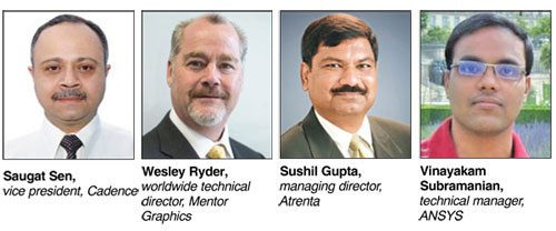
EFY catches up with four EDA firms to get their views on the latest in-chip design. Saugat Sen, vice president, Cadence; Wesley Ryder, worldwide technical director, Mentor Graphics; Sushil Gupta, managing director, Atrenta and Vinayakam Subramanian, technical manager, ANSYS, share their views on topics ranging from the latest transistor structures and their impact on EDA tools, to solving ASIC design challenges, important EDA concerns in chip design and the latest trends in this field.

Q. What has been the impact of the latest transistor structures on EDA tools?
Saugat Sen: FinFET is the latest transistor structure and is amongst the most radical technologies developed in the semiconductor industry in the last few decades. This technology offers power and performance advantages over the existing planar transistors. However, it requires new design rules and tools, and hence, presents a challenging task for the designer, especially at 20nm, 14nm and 10nm nodes. The device level models for FinFETs have now largely stabilised. The 3D elements of device extraction have been completed and calibrated.
Wesley Ryder: Advanced processes at 20nm and beyond, and the arrival of FinFET technology, bring with them the promise of significant performance and power consumption benefits—especially regarding leakage of power. Double patterning (DP) is a technique used to help overcome the constraints of the current 193nm wavelength lithography. The use of DP adds significant complexity and cost to IC design and manufacturing that goes beyond the basic cost of extra masks and manufacturing steps. With DP, any slight misalignment of the two masks can cause significant variability in the parasitics resulting from adjacent geometries.
Sushil Gupta: There are basically two forces at play here. On the one hand, advanced transistor structures present new challenges in areas such as power (leakage), process corner behaviour (variability) and lithography (printability). These require detailed characterisation of the transistor structures in order to develop models that can accurately reflect behaviour all the way through the design flow. On the other hand, the physical size of these structures gives rise to higher density and, thus, higher complexity for system-on-chip (SoC) design.
Vinayakam SUbramaniam: With the advent of FinFET technology, EDA power integrity analysis tools need to support the new transistor structures/parameters, like fins in the advanced SPICE models for accurate SPICE modelling/characterisation. Electro-migration (EM) rules are also becoming complex, and EDA tools need to support these complex EM rules for 16nm FinFET designs. Increased power density and lower supply voltage will cause reduction in the noise margin, making power integrity analysis more critical.
Q. What are some of the lesser known challenges encountered while designing ASICs?
Saugat Sen: ASICs are increasingly being used in consumer electronics where low power is one of the most critical factors. At nodes 45nm and lower, the issue is leakage, and to address this, designers use power-reduction techniques such as power gating, multi-supply voltage and clock gating. At lower nodes, due to the interconnect delays, timing closure between synthesis and layout presents a huge challenge for design engineers. The signal integrity, especially at advanced nodes, is affected by interconnect parasitics. The layout extraction method is one of the popular tools used by ASIC designers to overcome the issue.
Wesley Ryder: Issues like electrostatic discharge (ESD) and multiple power domain checks are high on the list of complex new geometrical and electrical verification requirements for modern SoCs. These requirements can be best described with a topological view rather than a device pin-to-net relation. In complex designs, sophisticated ESD protection device structures have to be verified. Usually, these structures are formed from a group of devices to construct better ESD prevention circuitry. Advanced programmable electrical rule checking (PERC) helps overcome these challenges. On the topological side, this allows the user to identify circuit elements that make up the ESD protection or low-power-related structures.
Sushil Gupta: I would say one of the most challenging aspects is successful IP selection and reuse. For many designs today, over 80 per cent of the chip is composed of previously designed IP, either legacy code or internally/externally sourced code. There are plenty of stories about schedule delays and design-closure challenges for these types of designs. In many cases, the root cause of those issues was improper selection of IP blocks, or selection of IP blocks with built-in ‘problems’ that get discovered too late in the design process. A more focussed and systematic approach to IP management and re-use would help a lot.
Vinayakam SUbramaniam: Reliability aspects like ESD and electro-migration tend to be overlooked, especially with respect to timing analyses. As we move to advanced technology nodes, electro-migration becomes more important due to degraded EM limits. From an ESD point of view, we see current density violations happening more frequently during ESD discharge events, leading to metal breakdown inside the chip.


