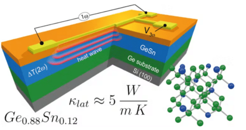
Researchers from Germany, Italy, and the UK have significantly advanced on-chip energy harvesting materials compatible with CMOS chip production.

The increasing use of electronic devices leads to higher energy consumption, released as low-temperature heat. Unfortunately, harnessing this low-grade heat, typically below 80°C, is challenging due to poor thermodynamic efficiency and technological constraints. Moreover, few materials can convert this heat into electrical energy and are compatible with existing semiconductor technologies, making direct utilization in computer processors difficult.
A collaborative effort involving Forschungszentrum Jülich and IHP—Leibniz Institute for High-Performance Microelectronics in Germany, the University of Pisa, the University of Bologna in Italy, and the University of Leeds in the UK has achieved a milestone in developing materials for on-chip energy harvesting. These materials are compatible with the CMOS chip production process, marking significant progress.
A thermoelectric element transforms temperature differences directly into electrical energy. When a temperature gradient exists across thermoelectric material, it prompts a flow of charge carriers, thus generating electricity. This mechanism is utilized to capture and recycle waste heat from electronic devices, converting it back into usable energy, thereby decreasing overall energy consumption.
A lower thermal conductivity is advantageous for efficient energy conversion in thermoelectric materials, as it maintains a larger temperature gradient. GeSn alloys are particularly effective because their reduced thermal conductivity facilitates a more pronounced gradient, improving their thermoelectric performance.
Group IV elements, often called the silicon group, are fundamental to all electronic devices. Utilizing their alloying capabilities, these elements are now broadening their applications to encompass thermoelectrics, photonics, and spintronics. The ambitious long-term objective for silicon-based technology is the monolithic integration of photonics, electronics, and thermoelectrics on a single chip. This integration aims to enhance device performance and foster the development of more sustainable technologies.
The researcher aims to advance the material by broadening the alloy composition to include SiGeSn and, ultimately, the Group IV alloy CSiGeSn and construct a functional thermoelectric device. This device will serve to demonstrate the energy-harvesting capabilities of Group IV alloys.


