It overcomes key barriers in chip design, offering a pathway to more powerful and compact electronics, critical for the growing demands of 5G and AI technologies.
A development in transistor technology could soon extend smartphone battery life and enable further advancements in miniaturized electronics. A collaborative team of electrical and computer engineers from the Shanghai Institute of Microsystem and Information Technology (Chinese Academy of Sciences), City University of Hong Kong, and Fudan University has engineered a new two-dimensional, low-power-consumption field-effect transistor (FET). The research, published in *Nature*, overcomes significant challenges that have hindered the creation of smaller, more efficient computer chips.
The team focused on resolving the issues of high gate leakage and low dielectric strength—two major obstacles that have prevented the effective miniaturization of silicon-based FETs. This innovation holds the potential to integrate more features into smartphones and other electronic devices without increasing their size, a critical requirement as the demand for more powerful 5G and AI-enabled devices grows. As the Internet of Things (IoT) continues to expand, the necessity for smaller and more efficient devices has become increasingly apparent. However, the materials traditionally used in these transistors have begun to encounter limitations, particularly with short-channel effects that impair performance. The search for new materials has led many in the field to explore two-dimensional (2D) materials, which offer the promise of reducing transistor thickness to just a few atoms.

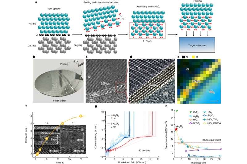
Previous attempts to utilize 2D materials have faced difficulties in achieving smooth integration with other essential components. However, the research team has made significant strides by using single-crystalline aluminum oxide, an ultrathin metal oxide just 1.25 nm thick, as a dielectric. The FETs they developed feature aluminum gates measuring 100 µm wide and 250 nm long, with a strategically designed gap between them to ensure complete insulation.
The researchers used standard van der Waals transfer methods to align the materials on the underlying wafer, creating a 2D FET with high-quality dielectric interfaces. This innovation could be a significant step forward in the ongoing quest for smaller, more efficient electronic components.