PSpice is central to the 5G transformation, offering powerful simulation capabilities that act as a secret weapon for fine-tuning BJT circuits to excel in the high-speed 5G environment.
After 1G, 2G, 3G, and 4G networks, the fifth generation 5G is a new global wireless standard extending beyond mobile communication to facilitate all forms of communication applications. 5G networks operate on different frequency bands. The low-frequency band is 1 GHz, the midband is 1 to 6 GHz, and the high-frequency band is 24GHz and higher. They offer numerous advantages regarding coverage, transmission speed, and handling capability. Many chip-making companies are developing linear power amplifiers and 5G millimetre wave transceiver semiconductor components at 1.8GHz, 2.6GHz, and 3.5GHz for use in the base stations of 5G mobile communications.
A preamplifier circuit pre-amplifies a feeble small signal to a suitable/compatible level that is fed to an attached power RF amplifier circuit in the (1Ghz-6Ghz) conventional 5G technology. With the use of high-speed internet, there is the possibility of uninterrupted communication between business operations (employer and customer). With 5G deployment, extra demand for bandwidth could be achieved.
Small antennas at repeaters in cell 5G networks are used to fix and relay signals. Spectrums range from (i) 3.3-3.8GHz for most commercial networks, and (ii) Other bands such as 1800MHz, 2.3GHz, and 2.6GHz are assigned for 5G with operator intervention. Considering a circuit with linear circuit elements and a non-linear device (bipolar junction transistor), the bias for the BJT is varied using Spice/PSpice DC sources, thus obtaining different base, collector, emitter voltages and collector currents.
Simulation method
Thevenin and Norton’s equivalent of networks containing a non-linear electronic device BJT (bipolar junction transistor) is obtained using the PSpice simulation analysis program.
Different networks for different operating points of BJTs are obtained along the equivalents in the frequency domain, and the results are used to acquire a new circuit with the same parameters to drive a known load.
A Thevenin equivalent circuit for the network (Fig: 1), and aNorton equivalent circuit for the same is obtained.
The individual Thevenin open circuit voltages are obtained for Fig:1 using Spice/PSpice files Table I. The individual Thevenin impedances are also computed using Figs: 1a and b
.
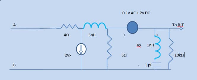
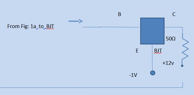
Figs: 1c and 1d show the DC nonlinear characteristics of the bipolar high-frequency transistor used in the simulations.
Thevenin open-circuit voltage is determined at both DC and AC voltages. Two different methods are used to determine Thevenin impedance at DC, with no change in the operating point of the non-linear device. The Norton short circuit value at DC is obtained by analogue behavioural modelling of PSpice. The Norton short circuit AC values are obtained carefully by maintaining the same bias at the non-linear device.
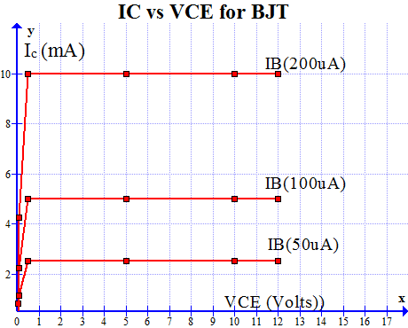
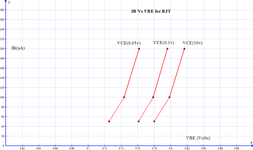
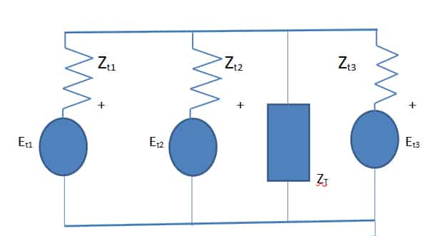
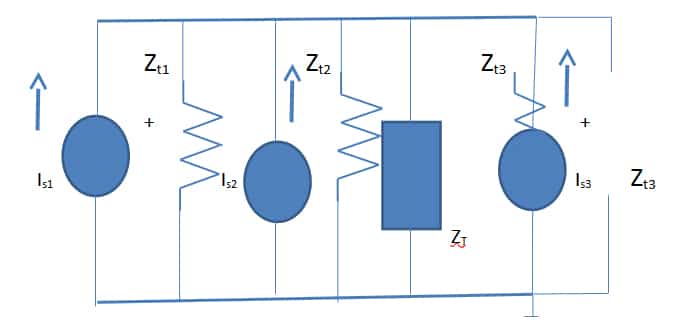
The Tables I and II describe the Spice/PSpice procedure to obtain Thevenin/Norton equivalents at DC (single bias of the non-linear device). The values are also verified with a practical circuit.
Table I: A method to obtain DC equivalent Thevenin resistance
| **** 09/25/23 14:10:33 ****** PSpice Lite (October 2012) |
| ****** ID# 10813 **** |
| Thevenin and Norton circuit determination with bias |
| **** Circuit description********** |
| .SUBCKT TN 1 6 7 |
| VIN 3 4 DC 2V AC 0.1V |
| R12 1 2 4 |
| R10 1 0 1E17 |
| G20 2 0 4 0 2 |
| L23 2 3 3NH |
| R30 3 0 5 |
| L45 4 5 1NH |
| C50 5 0 1PF |
| R40 4 0 10K |
| * Non-linear device description |
| Q2 6 4 7 0 QM |
| R2628 6 8 50 |
| V310 8 0 DC 12 |
| .MODEL QM NPN(IS=2E-16 BF=50 BR=1 RB=5 RC=1 RE=0 |
| CJE=0.4PF VJE=0.8 ME=0.4 CJC=0.5PF VJC=0.8 CCS=1PF) |
| .ENDS TN |
| X1 1 6 7 TN |
| V270 7 0 DC -1.05V |
| ET1 1 15 26 0 1 |
| ETX 29 0 1 15 1 |
| FO17 0 15 VX1 0.0001 |
| EXX 24 29 15 0 1E4 |
| VX1 20 24 |
| X4 26 27 28 TN |
| V260 28 0 DC -1.05V |
| R200 20 0 100 |
| .OP |
| .end |
| **** 09/25/23 14:10:33 ****** PSpice Lite (October 2012) |
| ****** ID# 10813 **** |
| Thevenin and Norton circuit determination with bias |
| **** Small signal bias solution Temperature = 27.000 DEGC************** |
| Node voltage |
| ( 1) 1.8176 ( 6) 9.0491 ( 7) -1.0500 ( 15)-7.739E-06 |
| ( 20) 1.7403 ( 24) 1.7403 ( 26) 1.8177 ( 27) 9.0490 |
| ( 28) -1.0500 ( 29) 1.8177 ( X1.2) 1.8177 ( X1.3) 1.8177 |
| ( X1.4) -.1823 ( X1.5) -.1823 ( X1.8) 12.0000 ( X4.2) 1.8177 |
| ( X4.3) 1.8177 ( X4.4) -.1823 ( X4.5) -.1823 ( X4.8) 12.0000 |
| Voltage source currents |
| Name Current |
| V270 6.020E-02 |
| VX1 -1.740E-02 |
| V260 6.020E-02 |
| X1.VIN 1.162E-03 |
| X1.V310 -5.902E-02 |
| X4.VIN 1.162E-03 |
| X4.V310 -5.902E-02 |
| Total power dissipation 1.54E+00 watts |
| **** 09/25/23 14:10:33 ****** PSpice Lite (October 2012) |
| ****** ID# 10813 **** |
| Thevenin and Norton circuit determination with bias |
| **** Operating point information Temperature = 27.000 |
| DEG C |
| ****************************************************** |
| ************************ |
| **** Voltage-controlled current sources |
| Name X1.G20 X4.G20 |
| I-source -3.647E-01 -3.647E-01 |
| **** Voltage-controlled voltage sources |
| Name ET1 ETX EXX |
| V-source 1.818E+00 1.818E+00 -7.739E-02 |
| I-source 1.740E-06 -1.740E-02 -1.740E-02 |
| **** Current-controlled current sources |
| Name FO17 |
| I-source -1.740E-06 |
| **** Bipolar junction transistors |
| Name X1.Q2 X4.Q2 |
| Model X1.QM X4.QM |
| IB 1.18E-03 1.18E-03 |
| IC 5.90E-02 5.90E-02 |
| VBE 8.68E-01 8.68E-01 |
| VBC -9.23E+00 -9.23E+00 |
| VCE 1.01E+01 1.01E+01 |
| BETADC 5.00E+01 5.00E+01 |
| GM 2.28E+00 2.28E+00 |
| RPI 2.19E+01 2.19E+01 |
| RX 5.00E+00 5.00E+00 |
| RO 1.00E+12 1.00E+12 |
| CBE 7.72E-13 7.72E-13 |
| CBC 2.17E-13 2.17E-13 |
| CJS 1.00E-12 1.00E-12 |
| BETAAC 5.00E+01 5.00E+01 |
| CBX/CBX2 0.00E+00 0.00E+00 |
| FT/FT2 3.67E+11 3.67E+11 |
| Job concluded |
Table II: Computation of DC equivalent Thevenin network and
| **** 09/25/23 12:43:30 ****** PSpice Lite (October 2012) |
| ****** ID# 10813 **** |
| Thevenin and Norton circuit determination with bias |
| **** Circuit description*********** |
| ************************ |
| .SUBCKT TN 1 6 7 |
| VIN 3 4 DC 2V AC 0.1V |
| R12 1 2 4 |
| R10 1 0 1E17 |
| G20 2 0 4 0 2 |
| L23 2 3 3NH |
| R30 3 0 5 |
| L45 4 5 1NH |
| C50 5 0 1PF |
| R40 4 0 10K |
| * Non-linear device description |
| Q2 6 4 7 0 QM |
| R2628 6 8 50 |
| V310 8 0 DC 12 |
| .MODEL QM NPN(IS=2E-16 BF=50 BR=1 RB=5 RC=1 RE=0 |
| CJE=0.4PF VJE=0.8 ME=0.4 CJC=0.5PF VJC=0.8 CCS=1PF) |
| .ENDS TN |
| X1 1 6 7 TN |
| V270 7 0 DC -1.05V |
| ET1 1 15 26 0 1 |
| ETX 29 0 1 15 1 |
| IFO17 0 15 DC 0.000001 |
| EXX 24 29 VALUE= {I(VX1)*1E6*V(15)} |
| VX1 20 24 |
| X4 26 27 28 TN |
| V260 28 0 DC -1.05V |
| R200 20 0 100 |
| .OP |
| .end |
| **** 09/25/23 12:43:30 ****** PSpice Lite (October 2012) |
| ****** ID# 10813 **** |
| Thevenin and Norton circuit determination with bias |
| **** Small signal bias solution Temperature = 27.000 DEG |
| ****************************************************** |
| ************************ |
| Node Voltage |
| ( 1) 1.8177 ( 6) 9.0490 ( 7) -1.0500 ( 15) 4.447E-06 |
| ( 20) 1.7403 ( 24) 1.7403 ( 26) 1.8177 ( 27) 9.0490 |
| ( 28) -1.0500 ( 29) 1.8177 ( X1.2) 1.8177 ( X1.3) 1.8177 |
| ( X1.4) -.1823 ( X1.5) -.1823 ( X1.8) 12.0000 ( X4.2) 1.8177 |
| ( X4.3) 1.8177 ( X4.4) -.1823 ( X4.5) -.1823 ( X4.8) 12.0000 |
| Voltage source currents |
| Total power dissipation 1.54E+00 WATTS |
| Job concluded |
The individual short circuit currents and Norton impedances for Figs: 2 and 3 are obtained using the Spice/PSpice file. They are added and stored using PSpice with circuit commands.
Table III: Spice/PSpice File for the circuit of Fig: 2
| **** 09/26/23 18:32:22 ****** PSpice Lite (October 2012) ****** ID# 10813 **** |
| Thevenin and Norton circuit determination with bias |
| **** Circuit description |
| *********************************************************************** |
| .SUBCKT TN 1 6 7 |
| VIN 3 4 DC 2V AC 0.1V |
| R12 1 2 4 |
| R10 1 0 1E17 |
| G20 2 0 4 0 2 |
| L23 2 3 3NH |
| R30 3 0 5 |
| L45 4 5 1NH |
| C50 5 0 1PF |
| R40 4 0 10K |
| * Non-linear device description |
| Q2 6 4 7 0 QM |
| R2628 6 8 50 |
| V310 8 0 DC 12 |
| .MODEL QM NPN(IS=2E-16 BF=50 BR=1 RB=5 RC=1 RE=0 CJE=0.4PF VJE=0.8 ME=0.4 CJC=0.5PF VJC=0.8 CCS=1PF) |
| .ENDS TN |
| X1 1 6 7 TN |
| V270 7 0 DC -1.05V |
| ET1 1 15 26 0 1 |
| ET2 9 0 FREQ {V(23)} = (1GHz,-9.043,74.28) (2GHz,-3.3315,81.15) (6GHz,6.035,88.85) |
| ET3 12 0 FREQ {V(23)} = (1GHz,-9.001,74.75) (2GHz, -3.213, 81.65 ) (6GHz, 6.195,88.91) |
| R90 9 0 1 |
| R120 12 0 1 |
| ETX1 29 0 1 15 1 |
| C2918 29 18 1 |
| ETX2 21 0 9 0 1 |
| ETX3 25 0 12 0 1 |
| FO17 0 17 VX1 1 |
| R170 17 0 1E23 |
| C1517 15 17 1 |
| EXX 19 18 17 0 1 |
| VX1 20 24 |
| R2419 24 19 0.000001 |
| E2021 20 21 FREQ {I(E2021)} = (1GHz,13.27,23.77) (2GHz,14.74,46.67) (6GHz,23.36,61.64) |
| E2022 20 22 FREQ {I(E2022)} = (1GHz, 13.38,21.82) (2GHz,14.52,41.52) (6GHz,22.37,57.51) |
| R2225 22 25 0.0000001 |
| R200 20 0 1K |
| VC1 23 0 AC 1 |
| R230 23 0 1 |
| X4 26 27 28 TN |
| V260 28 0 DC -1.05V |
| .AC LIN 6 1GHz 6GHz |
| .PRINT AC VDB(1) VP(1) VDB(9) VP(9) VDB(12) VP(12) |
| .PRINT AC VM(20) VP(20) |
| .PRINT AC VM(29) VP(29) VM(1,15) VP(1,15) |
| .PRINT AC VM(20) VP(20) |
| .OP |
| .end |
| FREQ VM(20) VP(20) |
| 1.000E+09 3.498E-01 7.408E+01 |
| 2.000E+09 6.765E-01 8.121E+01 |
| 3.000E+09 1.007E+00 8.333E+01 |
| 4.000E+09 1.333E+00 8.484E+01 |
| 5.000E+09 1.586E+00 8.794E+01 |
| 6.000E+09 1.993E+00 8.874E+01 |
| **** 09/26/23 18:32:22 ****** PSpice Lite (October 2012) ****** ID# 10813 **** |
| Job concluded |
Table IV: Spice/PSpice file for simulating Fig: 3 networks
| **** 09/26/23 18:48:17 ****** PSpice Lite (October 2012) ****** ID# 10813 **** |
| Norton AC circuit determination with bias |
| **** Circuit description |
| *********************************************************************** |
| .SUBCKT TN 1 6 7 |
| VIN 3 4 DC 2V AC 0.1V |
| R12 1 2 4 |
| R10 1 0 1E17 |
| G20 2 0 4 0 2 |
| L23 2 3 3NH |
| R30 3 0 5 |
| L45 4 5 1NH |
| C50 5 0 1PF |
| R40 4 0 10K |
| *Non-linear device description |
| Q2 6 4 7 0 QM |
| R2628 6 8 50 |
| V310 8 0 DC 12 |
| .MODEL QM NPN(IS=2E-16 BF=50 BR=1 RB=5 RC=1 RE=0 CJE=0.4PF VJE=0.8 ME=0.4 CJC=0.5PF VJC=0.8 CCS=1PF) |
| .ENDS TN |
| X1 1 6 7 TN |
| C135 1 35 1E14 |
| V350 35 0 |
| X2 36 37 38 TN |
| V380 38 0 DC -1 |
| C3639 36 39 1 |
| V390 39 0 |
| X3 40 41 42 TN |
| V420 42 0 DC -0.95V |
| C4043 40 43 1 |
| V430 43 0 |
| R2419 24 19 0.000001 |
| E2021 20 0 FREQ {I(E2021)} = (1GHz,13.27,23.77) (2GHz,14.74,46.67) (6GHz,23.36,61.64) |
| E2022 20 22 FREQ {I(E2022)} = (1GHz, 13.38,21.82) (2GHz,14.52,41.52) (6GHz,22.37,57.51) |
| R220 22 0 0.00001 |
| FO15 0 15 VX1 1 |
| EEX 19 0 15 0 1 |
| VX1 20 24 |
| C2419 24 19 1 |
| R200 20 0 1K |
| FF0020 0 20 V390 1 |
| FA0020 0 20 V430 1 |
| FB0020 0 20 V350 1 |
| X4 44 45 46 TN |
| V460 46 0 DC -1.05V |
| E4447 44 47 48 0 1 |
| C4415 47 15 1 |
| R150 15 0 1E23 |
| X5 48 49 50 TN |
| V500 50 0 DC -1.05V |
| .AC LIN 6 1GHz 6GHz |
| .PRINT AC VM(20) VP(20) IM(V350) IP(V350) VM(1,35) VP(1,35) |
| .OP |
| .end |
| Norton AC circuit determination with bias |
| 09/26/23 18:48:17 ****** PSpice Lite (October 2012) ****** ID# 10813 **** |
| Norton AC circuit determination with bias |
| **** AC analysis Temperature = 27.000 DEG C |
| *********************************************************************** |
| FREQ VM(20) VP(20) |
| 1.000E+09 3.498E-01 7.408E+01 |
| 2.000E+09 6.765E-01 8.121E+01 |
| 3.000E+09 1.007E+00 8.333E+01 |
| 4.000E+09 1.333E+00 8.484E+01 |
| 5.000E+09 1.586E+00 8.794E+01 |
| 6.000E+09 1.993E+00 8.874E+01 |
| Job concluded |
A possible application using dependent controlled voltage/current sources.
Application I: Spice models for dependent sources from DC to microwave frequency embed simulation In practical equivalent network ‘simulation’ for embedded circuits, four types of dependent sources (voltage-controlled voltage, voltage-controlled current, current-controlled voltage, current-controlled current) are obtained for transmittances and current/voltage ratios expressed as a combination of Laplace transforms and complex number algebra. Here, the controlling voltage/current is through a combination of immittances expressed as a function of Laplace transforms and complex numbers. Examples can be simulated results for very low and microwave frequencies up to 10GHz.
In this application, (a) two different networks (Fig: 4a) consisting of linear elements and dependent and independent sources are considered.
Two different controlled sources, (i) voltage-controlled voltage source in second network(N2) whose controlling voltage is across an impedance in first network(N1), represented by expressions in s domain and complex numbers in Cartesian form, (ii) voltage controlled current source in first network (N1) whose controlling current is across an impedance in second network (N2), represented by expressions in ‘s’ domain and complex numbers in Cartesian form.
Both the dependent sources are modelled using PSpice. (b) Another different linear network (N3) (Fig: 4b) consisting of a current-controlled voltage source and a current-controlled current source with controlling current, which are functions of the combination of expressions in the ‘s‘ domain and complex numbers expressed in polar form, in the same network, is simulated again using PSpice.

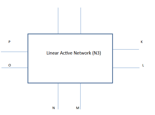
From the definition of equivalent circuits for four types of dependent sources, the various models when their conversion ratios (voltage/voltage, voltage/current, current/voltage, current/current) are expressed as a combination of functions of Laplace variables(s) and complex numbers are constructed using PSpice circuit analysis program ingeniously. The controlling variables for these dependent sources are from the same network or two different networks. An equivalent representation of control variables, which are again expressed in Laplace domain(s) and complex numbers, is obtained again with the PSpice program. The technique can be used with networks consisting of two ports of high-frequency theoretical small signal representation of circuits at microwave frequencies.
Final thoughts
The evolution from 4G networks to 5G technology transformed public life and industries by providing various opportunities for the innovation of radio frequency (RF), microwave, and millimetre wave components.
Spice/PSpice circuit simulation and analyses program has been used to obtain Thevenin/Norton equivalents for two new circuits having Thevenin/Norton voltages (for three different biases to non-linear device) and Thevenin/Norton impedances (for three different biases), driving a load. The DC Thevenin resistance for a circuit consisting of a non-linear device is obtained by a new method compatible with the PSpice simulation program.
The DC Thevenin resistance could be obtained from I Tables I and II by the formulas which are PSpice/Spice compatible, (a) v(15)/(1e-06*I(vx1)), (b) (v(24)-v(29))/I (vx1).
The DC short circuit Norton current is obtained by the analogue behavioural option or by simple division of Thevenin DC resistance with DC Thevenin/Norton resistance. A circuit with DC Thevenin/Norton resistances, with DC Thevenin voltage, is simulated and verified. In this circuit the DC Norton resistance is obtained by using a combination of V and I current relation in a branch. In recent years, field operators, engineers, and wireless network installers have replaced available spectrum analysers, giving solutions with the same quality measurement schemes as portable, battery-operated solutions with less weight and size.


