Researchers achieved a precise fabrication method of 2D semiconductors for CMOS inverters array.

A team of researchers from Peking University, China have created a method for precisely doping two-dimensional (2D) semiconductors. Using substitutional doping, the team successfully synthesised thin films of 2H-MoTe2 with P-type and N-type regions, enabling the fabrication of a chip-sized 2D CMOS inverter array. This achievement represents a significant step toward revolutionising integrated circuit technology.
Precise doping plays a critical role in semiconductor fabrication, determining the conductivity and functionality of devices. While traditional doping methods like ion implantation are well-suited for bulk materials such as silicon, they are incompatible with atomically thin 2D semiconductors. This study overcomes that limitation, demonstrating a scalable approach to doping 2D materials with unparalleled precision.
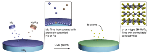
The researchers used magnetron sputtering and chemical vapour deposition techniques to incorporate niobium (Nb) and rhenium (Re) into 2H-MoTe2 films. The resulting P- and N-type channels were then used to construct back-gate and CMOS devices. Hall measurements revealed distinct doping characteristics: Nb-doped films exhibited p-type behaviour, while Re-doped films displayed ambipolar and N-type characteristics, depending on doping levels. These findings confirm the high-quality synthesis and controlled carrier concentrations of the doped films.
This innovation targets semiconductor manufacturers and researchers exploring next-generation electronics. The compatibility of the method with large-scale fabrication was demonstrated by producing hundreds of CMOS inverter arrays on centimetre-scale chips. By achieving reproducible doping and integrating P- and N-type films, the study highlights the potential for scalable production of advanced electronic devices.
“This method allows for spatially selective doping with remarkable accuracy, paving the way for high-performance integrated circuits,” the researchers noted. Their work also demonstrated the stability of the doping process and the uniformity of electrical performance across multiple devices, underscoring its practical applicability.
The versatility of these doped films extends beyond conventional applications. They can integrate seamlessly with various substrates and enable interlayer connections, offering new possibilities for monolithic silicon chip designs. This transformative approach could accelerate the development of ultra-compact, energy-efficient electronics while advancing fields like artificial intelligence and quantum computing.


