UC Santa Barbara researchers have developed a new framework to create scalable 3D transistors using 2D semiconductors, considering key factors that impact performance.

Silicon-based electronics are reaching their limits in performance and scalability. Engineers have been exploring new designs to make electronic components smaller, faster, and more energy-efficient to address this.
Researchers at the University of California, Santa Barbara, have developed a framework for creating scalable 3D field-effect transistors (FETs) using 2D layered semiconductors. Their approach considers factors like Schottky contact effects and inclusive capacitance, which influence transistor performance.
The team aimed to show the potential of atomically thin 2D materials for building next-generation 3D FETs with different architectures. They also sought to identify the best materials, designs, and architectures for these transistors.
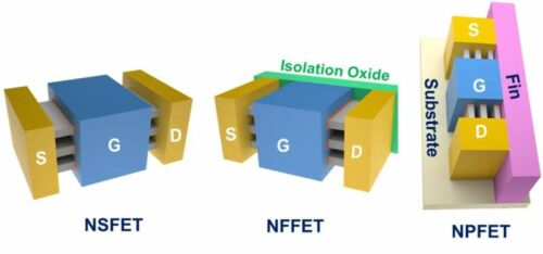
During their study, the researchers found that 2D materials could be uniquely engineered to create a new transistor architecture called the nano-plate FET (NPFET). This design offers improved performance and higher integration density.
The researchers used a practical mass-based approach for different versions of the NEGF function. This method proved efficient and accurate while also considering energy-band non-parabolicity, satellite valleys, and the finite energy width of these valleys.
Simulations by the researchers indicate that 3D FETs made with 2D semiconductors outperform silicon-based FETs. The channel length of these 2D material-based FETs was reduced to about 7 nm or less, with WS2 showing the best results.
The NPFET architecture developed by the team uses the thinness and vertical stacking of 2D semiconductors to scale transistors. Compared to earlier 3D-FET designs, this architecture offers significant integration density and performance advantages.
The researchers plan to collaborate with industry partners to accelerate the integration of these materials and designs into mainstream CMOS processes. They also intend to improve their simulations by including a wider range of non-ideal effects, such as defect scattering and self-heating, to provide deeper insights and support experimental advancements in the field.
Reference: Arnab Pal et al, Three-dimensional transistors with two-dimensional semiconductors for future CMOS scaling, Nature Electronics (2024). DOI: 10.1038/s41928-024-01289-8.


