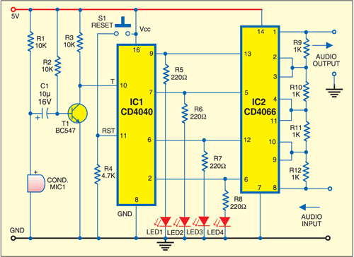
 This clap-based digital volume control offers four levels of volume control. With each clap, the volume of the audio system increases. After the fourth clap, the level of volume returns to the first or minimum level.
The circuit consists of a microphone, a level detector, a 4-stage counter and four analogue switches connected to a resistive ladder network.
The four outputs of the CD4040 counter are available at pins 9, 7, 6 and 2. These outputs are connected to the level detector formed by LED1 through LED4 and control input pins 13, 5, 12 and 6 of IC CD4066 quad bilateral switch. Resistors R9 through R12 form the ladder network.
The circuit is powered by regulated 5V and consumes only a few milliamperes of current. The audio input signal from sources such as MP3 player and PC is fed to pin 8 of CD4066. The output of the circuit is taken from pin 1 of CD4066 and can be fed to any audio power amplifier.

The clapping signal captured by the electret microphone (MIC1) is amplified by transistor T1. MIC1 gets its bias voltage through resistor R1.
Counter IC CD4040 (IC1) gets a clock pulse at its pin 10 when a certain noise level (threshold) is received through T1. The counter output determines the configuration of the four electronic switches inside IC2.
When output pin 9 of IC1 goes high, control pin 13 of IC2 shorts its pins 1 and 2, bypassing resistor R9 in the audio output line. Similarly, control pins 5, 12 and 6 of IC2 bypass resistors R10, R11 and R12, respectively. Thus, as per the sequential output across IC1, the series resistors are effectively introduced or removed in the audio output signal line. The maximum audio output is obtained when resistors R9 through R12 are shorted. The level of the audio signal can be seen on the LEDs (LED1 through LED4), with LED4 showing the maximum level.
Switch S1 allows the counter to reset, thus switching off all the switches of CD4066. In this case, attenuation in the audio output path is maximum as none of resistors R9 through R12 is shorted.
To calibrate the circuit, disconnect the clock input (pin 10) of CD4040 from the collector of T1. Now apply a pulse to the clock input by briefly connecting it to the +5V line. You will see the counter outputs change the state sequentially and so also the bilateral switches in CD4066.


how to get mic in proteus software?
thanks in advance