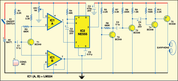
 Normally, hearing aid circuits consume battery power continuously once they are switched on. The smart hearing aid circuit given here saves battery power by switching on the sound amplifier section only when sound is detected. The sensitivity of the detection section and the ‘on’ time duration of the sound amplifier circuit can be set by the user. Also the circuit uses only a single condenser mic for sound detection and amplification.
A Smart Hearing Aid
As is clear from the above, this hearing aid consists of a condenser microphone, earphone, and sound detection and amplification sections. The sound detection section employs a quad op-amp IC LM324 (IC1(A)) and a timer NE555 (IC2). The sound signal received at the mic is pre-amplified by transistor BC549 (T1). The voltage at its collector is fed to the inverting terminal (pin 2) of op-amp IC1(A), which is used as a comparator. The reference voltage (Vref) at the non-inverting terminal (pin 3) of IC1(A) is set using preset VR1. The preset is also used to control the sensitivity of the sound signals received by the circuit. The output from pin 1 of IC1(A) is fed to the trigger input (pin 2) of timer NE555, which is configured in monostable mode.
Hearing aid circuit

When sufficient sound signal strength is detected at the base of transistor T1, the pulsating voltage at its collector exceeds the reference voltage at pin 3. As a result, output pin 1 of IC1(A) goes low. The low output from IC1(A) triggers the NE555 timer and its output goes high for a preset duration. R4 and C2 are the timing components for setting the time duration. The high output of the timer is directly used as the power source for the sound amplifier section.
Sound Amplifier
The sound amplifier section is built around transistors T2 through T5. The last amplifier stage T5 (pnp transistor BC558) drives the earphone. The sound signal received from the mic is fed to the non-inverting pin of the second op-amp of IC1(B) which is wired in unity follower configuration. The unity follower mode resolves the problem of impedance mismatch which would have occurred if the output of the mic is fed directly to amplifier stage. The output from pin 7 of IC1(B) is fed to the base of transistor T2. The weak signal received at transistor stage T2 is further amplified by transistors T3, T4 and T5. An earphone to listen to the sound is connected between the collector of T5 and ground. It is recommended to use a mono earphone with volume control attached.
Circuit Operation
With 9V DC supply, when sound is detected through the mic, the amplifier section is automatically triggered and the current consumption of the circuit is about 96 mA. When the amplifier circuit is ‘off,’ the circuit draws a current of about 6 mA only, thus saving considerable amount of battery power.
The article was first published in March 2009 and has recently been updated.


Hai sir/madam,
while connecting this circuit,in the sound amplification section employed with T2,T3,T4,T5 transistors.in that part the DMM voltage is obtained at T4 transistor only (T5,T3,T2 are not getting the voltage levels).
please suggest any solution….
Hearing aids have very few parts 1.mic.2.IC .3 speaker 4.battery.5.miscellanous like tube casing etc.However there are very few manufacturer in India.Most are imported from u.s and Europe.
Since only two op amps are needed, better to use the LM358, which is identical to the LM324 but has only two op amps. The LM324 has 4 op amps but two are not needed for this circuit.
1) The LM324 is a useless IC as far as audio use is concerned. Moreover, it is a quad op-amp, a 14-PIN DIP package which is very big for a hearing aid amplifier which should ideally have a small casing. An 8-PIN dual op-amp is the preferred IC in this case.
2) Use of a 9 volt battery is overkill, hearing aids should work with as low voltage as possible. A 1.5V cell is the most preferred battery, or a 3V lithium coin cell can also be used.
3) 96 mA of current drain is too much for a device which needs to be used continuously for long hours. Usually, good hearing aids have current drain in the range of 1 to 10 mA.
4) The worst feature of this circuit is the absence of a volume control.
These are my personal observations. Please do correct me if I am wrong. Thanks.