Listening to music on a self-made system is great. Good-quality audio amplifier circuits can be constructed with minimum components. Described here is an LME49710 based audio amplifier. Author’s prototype is shown in Fig. 1.
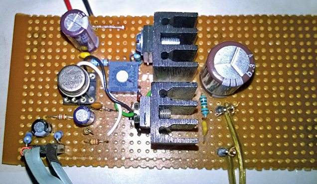
LME49710 based audio amplifier circuit
As shown in Fig. 2, the circuit diagram of the LME49710 based power amplifier consists of power supply unit and audio amplifier unit.
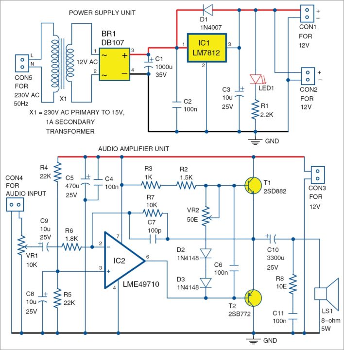
The power supply unit is a linear type built around transformer X1, bridge rectifier DB107 (BR1), 12V voltage regulator LM7812 (IC1) and a few other components. The 230V AC primary of X1 is stepped down to 15V, 1A. DB107 converts AC to pulsating DC, filtered with capacitors C1 and C2, and the rectified output is given to a 12V regulator (IC1). Diode 1N4007 (D1) is used to protect IC1 from reverse voltage. LED1 is used as the power indicator. Resistor R1 is used to limit the current passing through LED1.
The audio amplifier circuit is built around LME49710 (IC2), which is a high-performance, high-fidelity, audio-operational amplifier. The 12V power supply is connected to op-amp power pins. The single-supply operation requires a virtual ground at a voltage level of Vcc/2 = 12V/2 = 6V at the non-inverting terminal of op-amp IC2.
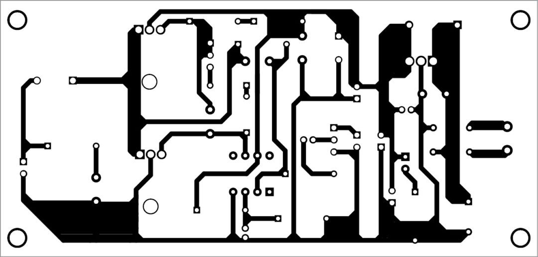
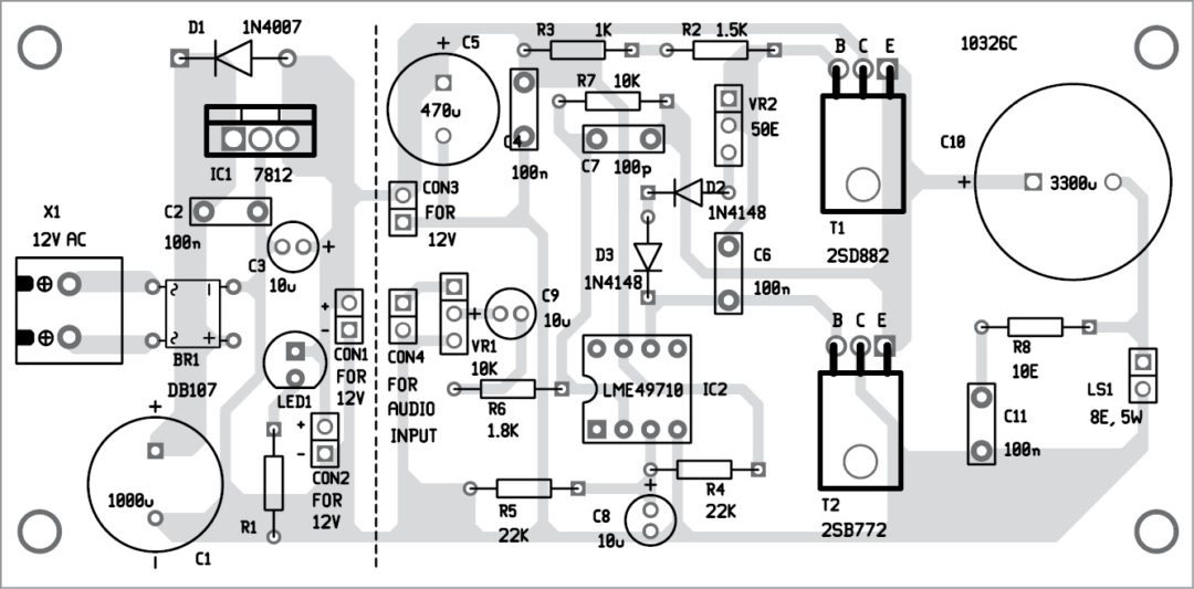
Download PCB and component layout PDFs: click here
The circuit can be constructed with a simple voltage divider formed by resistors R4 and R5 and bypassed by capacitor C8. Capacitors C4 and C5 decouple the noise at IC level, where C5 works as an electrolytic decoupling capacitor to reduce low- and mid-frequency noise and C4 reduces high-frequency noise in the power supply lines.
Audio input is connected at connector CON4. Capacitor C9 blocks DC voltage at input stage and potmeter VR1 controls the volume, up and down.
Resistors R7 and R6 set the gain of amplifier IC2. R7 and capacitor C7 limit the bandwidth of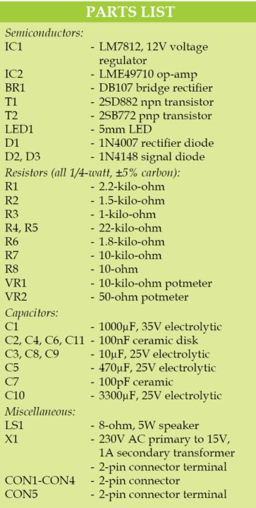 the amplifier and keep it linear, resistors R2 and R3 set the bias current of Vbe multiplier formed by diodes D2 and D3, and potmeter VR2 helps with bias current adjustment. Vbe multiplier is the DC bias voltage that overcomes turn-on base-emitter voltage drops of output transistors T1 and T2.
DC bias also keeps T1 and T2 active when no-load current is being delivered to the speaker or load. T1 and T2 drive the speaker through capacitor C10, which also blocks DC. Resistor R8 and capacitor C11 form a low-impedance path for the high-frequency noise that appears across speaker LS1.
Duplicate the same circuit for another channel to make it a stereo amplifier. The same power supply at CON2 may be used for the second amplifier unit.
Construction and testing
A single-side PCB for the LME49710 based audio amplifier is shown in Fig. 3 and its component layout in Fig. 4. Power supply and amplifier units are separated by dotted lines where right side of the PCB is for the audio amplifier unit. A similar PCB can be used for the second amplifier unit.
Fit VR1 and CON4 on the front side of the panel for volume control and audio input connections, respectively. Adjust VR2 to around 11 ohms. We have used 2-pin connector for audio input but you can use RCA female connector or stereo female socket for audio input and connect the music player/iPod/mobile. Enclose the setup in a small plastic box. Connect the transformer primary to 230V AC mains supply.
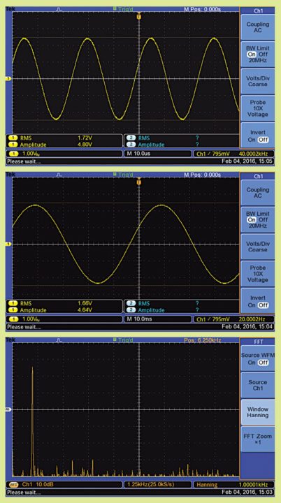
Fig. 5 shows the audio output wave forms seen in an oscilloscope with audio input taken from the function generator. The wave forms you see are measured across the load of 7.5 ohms.
Results
Output impedance: 0.01-ohm
Frequency response: flat from 20Hz – 40kHz
Total harmonic distortion: 1.2% at 3W peak
Test frequency: 1kHz sine of 1Vpp input
Can easily drive 3-ohm to 8-ohm speakers


can you make a 1000Watt amp using LME49710
Total harmonic distortion: 1.2%at 3W peak ?
LME49710 datasheets show a THD+N of only 0.00003%. What’s the use of a so good IC to obtain just 1.2% THD at 3W peak?
@Marc
THD+N = 0.00003% when the R_LOAD is 2Kilo-ohm, Here it is little overloaded, so the distortion is High, we can reduce it using multiple voltage driver amplifier and then followed by Power amplification.
Comment: what is the rms output of this amplifier ?
What changes need to be made in the circuit to get 40 watts ?
The author Visweswara Rao replies:
The circuit was designed to deliver less than 10watts RMS power, If you want to increase the audio power circuit should be modified with high power transistors, Proper bias, Voltage amplification stage (VAS) and power supply voltage should also be high minimum 50V to GND single power supply or 25-0-25 split power supply.
So what’s the rms output of this amplifier?
Please suggest suitable transistors to increase the power output to at least 20 watts
So, what’s the rms output of this amplifier?
Please suggest suitable transistors to increase the power to at least 20 Watts
HI.
https://s19.picofile.com/file/8440733668/2021_09_14.png