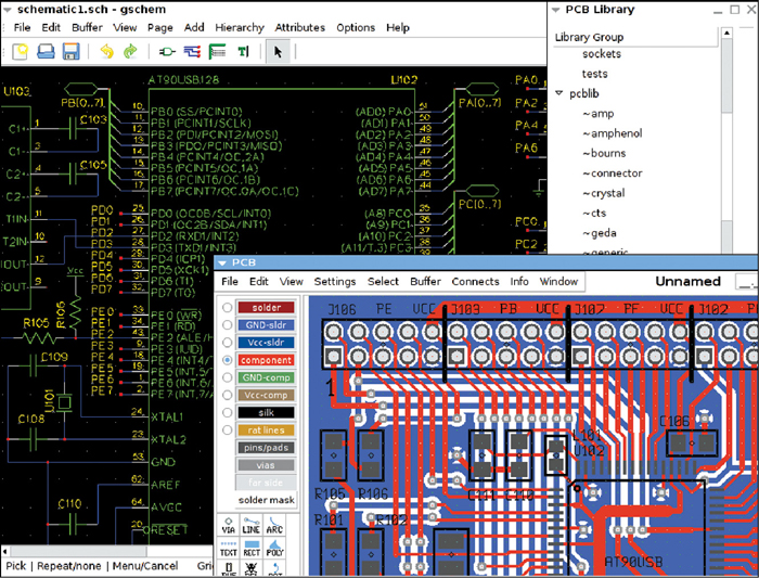
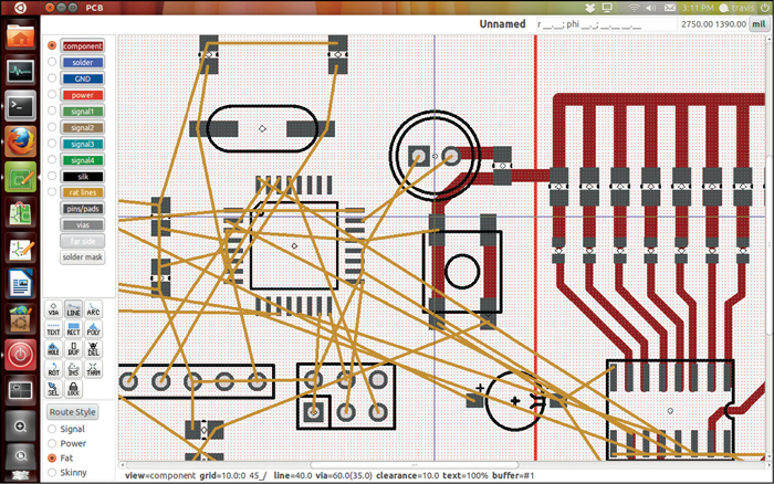
Electronic design automation (EDA or ECAD) is a category of software tool used to create, modify, analyse and optimise the designs of electronic systems. These tools assist the designer throughout the product design cycle and automate a lot of standard tasks to save time and energy, freeing designers to address more important challenges. EDA software increases the productivity of the designer, improves the quality of design, improves communication through documentation, and generates industry-standard output data directly for manufacturing.
How was it done in the old days?
Before the idea of EDA was conceived, the designs were laid out by hand. Some expert designers used geometric software to make layouts. The process was fundamentally graphic, with the translation from electronics to graphics done manually. By the mid-1970s, designers started automating the drafting of designs when tools for placement and routing came into existence.

But the major breakthrough occurred in 1980 with the publication of ‘Introduction to VLSI Systems’ by Carver Mead and Lynn Conway. This ground-breaking text advocated chip design with programming languages. This idea of using a programming language to define electronic components is the core of current-world EDA tools. The immediate result was a considerable increase in the complexity of the chips that could be designed, with improved access to design verification tools that used logic simulation.
How EDA tools increase productivity?
EDA tools increase productivity multi-fold. These tools support every phase of the product design cycle and make each task more organised, traceable and quick. When you want to design a new project, you start with making the schematic. Now, if you were to do this by hand you would have to draw each symbol manually, referring to the datasheet. You cannot remember the pin configuration of each component and most of the design cannot be completed in one day. This means that every time you come back to the project, you will be referring to the datasheets repeatedly for each component to draw symbols. Isn’t this cumbersome?
The EDA tools simplify such repetitive tasks with the help of a computer. Most of the symbols come built-in with EDA tools which you just have to select, place on the worksheet and connect with each other. And if some symbol is missing, it can be easily created and used in all future designs. The complete design itself can be simulated and checked for expected functionality, which reduces the chance of errors at later stages. Such organisation and automation, in turn, reduces human error and increases the overall productivity.

Now, to make the PCB of your design, you will have to draw it manually, corresponding to the schematic, if EDA tools were not available—something today’s designers cannot even imagine doing. It is highly unproductive and there are high chances of human error. With EDA tools, there is now a lot of automation involved for PCB design. You can import your design directly to the PCB tool and you will find all the footprints already connected with rat lines. These rat lines exactly correspond to the schematic’s wiring. This means that if your schematic is correct, the PCB will match it exactly. A lot of automation features like auto-routing, auto-placement, DRC (design rule check), etc, help in making the highest-quality, error-free PCBs.
Once the PCB is ready, you will have to send it to the PCB manufacturer for prototyping. With these EDA tools, the manufacturer and designer are in sync. The standard output data to manufacture the PCB can be easily generated. This is then directly fed to the machines for manufacturing. After you receive the PCBs, they will be sent to the assembler for the mounting of components. The Bill of material (BOM) and manufacturing data required by the assembler is created with just the click of a button and the chip shooter mounts the components in minutes. If you have to do all this manually, the time to market will be long, and the results uncertain.
Why is it important to select the right EDA tool?
While selecting an EDA tool, the first thing that you should keep in mind is that this tool will be used throughout the organisation by different departments. Therefore this tool should support the requirements of each department. You would not want to use several different tools because then, inter-departmental communication becomes impossible. So it is best that you consider the requirements of each department and chose the tool that suits them all or can be configured to do so.


