Despite huge efforts put in by electronics industry in the past 25 years, electrostatic discharge (ESD) still affects production yields to a great extent and in turn reduces profitability and product quality.


Various studies around the world reveal the fact that the reason for damage in 60-90 per cent of defective devices is ESD. Seventy per cent of these failures are attributed to damage caused by ungrounded people. The cost of damaged devices, shipping, repairs and rework can be so high that it consumes the entire profit margin of a project. It is highly unlikely that any organisation which ignores ESD safety will be able to successfully manufacture and deliver undamaged electronic products.
ESD susceptibility symbol. The well-known ESD cautionary symbol comprises a yellow hand in the act of reaching, crossed by a bar, all within a black triangle. It intends to identify devices and assemblies that are susceptible to ESD and so the personnel should be grounded when un-packaging or handling them. The symbol should be used on assemblies and devices that have sensitivity towards ESD.

ESD protection symbol. This symbol appears on ESD protective products such as shielding bags and boxes. The asterisk sign is replaced with a letter indicating the primary function of the item such as:
‘L’ for low-charging materials. These materials are also known as astatic or antistatic materials. Packaging using such material minimises charge generation by separation from or rubbing with other materials.
‘S’ for shielding materials that act as a barrier or an enclosure that limits the passage of current and attenuates the energy resulting from an ESD.
‘D’ for dissipative materials with surface resistance between 1×10⁶ ohm and 1×10¹² ohm.
‘C’ for conductive materials with a surface resistance between 1×10³ ohm and 1×10⁶ ohm.

ESD common point ground symbol. This symbol intends to notify people of an ESD common point ground. This common grounding point grounds all components of the work area such as work surfaces, staff and equipment to one common point, thereby reducing the risk of ESD.
Static electricity
 It is important to understand static electricity in order to prevent and control ESD. Static electricity is an imbalance of electric charges within or on the surface of a material. The charge remains until it is able to move away by means of an electric current or electrical discharge. ESD can change the electrical characteristics of a semiconductor device, degrade it or even destroy it completely. This static charge build up is majorly caused by tribocharging and electrostatic induction.
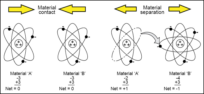
Tribocharging. Creation of electrostatic charge by contact and separation of materials is known as triboelectric charging. The atoms of a material without static charge have an equal number of protons in their nucleus and electrons orbiting the nucleus. The atom in this state is electrically neutral.
Fig. 1 shows two electrically neutral materials. When these materials are separated after contact, some negatively charged electrons get transferred from the surface of one material to the other. The material that loses electrons becomes positively charged, while the material that gains electrons becomes negatively charged.
Which material becomes negative and which becomes positive depends on the relative tendencies of the materials involved to gain or lose electrons. Some materials have a greater tendency to gain electrons than the others. Similarly, some materials tend to lose electrons easier than the others.
The triboelectric series (Table I) lists various materials according to their tendency to gain or lose electrons. It usually lists materials in order of decreasing tendency to charge positively (lose electrons), and increasing tendency to charge negatively (gain electrons).
Somewhere in the middle of the list are materials that do not show strong tendency to behave either way. Note that the tendency of a material to become positive or negative after triboelectric charging has nothing to do with the level of conductivity (or ability to discharge) of the material.
The charge created by triboelectric effect depends on various factors such as area of contact, the speed of separation, relative humidity and chemistry of the materials and surface work function. Table II shows the common charge generation situations and the resulting voltage levels generated due to static electricity.
The contribution of humidity in reducing charge accumulation is also known. It should be noted, however, that some static generation occurs even at high relative humidity. It is not recommended to have relative humidity that is too low, say, below 30 per cent. ESD control becomes especially challenging at low-RH levels. A relative humidity between 40 per cent and 60 per cent is recommended for a typical assembly area.


