The SiC and GaN semiconductor industry in India has seen a positive growth trend in the past couple of years. Many companies have shown their interest in investing in projects related to WBG semiconductor production in India, mainly due to increased market acceptance of WBG chips. WBG semiconductors can give an edge to the final system design of various power applications.
The wide-band-gap (WBG) semiconductor device landscape has seen quite an evolution over the past couple of decades.
We have seen innovative use of power devices evolve from the days of the mainframe computers in the sixties to the current IoT era. And this revolution in technology has seen the evolution of WBG semiconductor chips. WBG components have not only become easier to produce but have seen their applications grow multifold as they become more cost-efficient and deliver improved performance coupled with system size reduction—both highly coveted system design functionalities.
Still, the potential of WBG semiconductors is yet to be explored by the power electronics industry in India.

Why WBG semiconductors?
The most common WBG semiconductors, the silicon carbide (SiC) and gallium nitride (GaN) semiconductors, have become game changers in the semiconductor chip manufacturing industry and produced what may be termed as an ‘inflection point.’ 2020 has seen an explosive growth in GaN based mobile chargers!
Dr Ashwini Aggarwal, director at Applied Materials India, says, “The industry has discovered opportunities in the WBG semiconductors for specific types of power and RF applications. Some of these wideband semiconductors have very interesting properties which conventional silicon is not able to match.”
To begin with, SiC and GaN provide phenomenally higher bandgap energy when comparing the same with silicon.
But what is this bandgap energy?
It is the energy required to excite an electron from the valence band to the conduction band. If the bandgap is large, a higher critical field is required to initiate ionisation and create a free flow of electrons. To put it simply, a higher bandgap allows devices to function at higher temperatures. Conventional semiconductors tend to be notorious since their bandgap usually narrows down with an increase in temperature.
Additionally, devices operating on wide-bandgap semiconductors can also switch between higher voltages with ease. Since these have faster switching speeds and lower switching losses, they also have a higher switching frequency. This is another interesting aspect of WBG semiconductors.
This results in an inverse relationship between the size of the capacitor/inductor and the switching frequency. That is because these are energy storage devices. The energy that they store and pass on are linked, among other things, to the capacitors and the switching frequency. So, if the switching frequency increases, to get the same energy transmission or storage, the size of the capacitor or inductor will come down. For example, in a typical charger circuitry, the moment you use a gallium nitride power device the size of the charger will reduce dramatically.
Another key advantage that sets these chips apart is that they have a better thermal conductivity, which helps bring down their cooling needs exponentially. These are also known to be highly reliable, as well as durable.
Factors like these impact the device system’s functioning, size, and weight dramatically. Consequently, WBG semiconductors can give an edge to the final system design of various power applications.
Climate change is pushing for evolution in power electronics for better energy consumption and better efficiency, while digitisation is making it imperative to store more and more data, thereby increasing the need to accommodate more storage spaces with sufficient volume, efficiency, and cooling systems.
Here, too, WBG chips can help a business reduce its carbon footprint. Their role in climate change has already been recognised by many conventional power applications like wind, UPS, rail, and motor drives where they form an integral part of the system.

Manufacturing chain
The manufacturing process for a WBG semiconductor device involves the conventional device creation process.
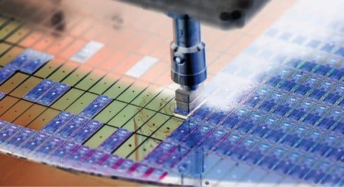
The first is the front-end process during which we first start with an ingot, slice it off using a laser or wire saw and then polish it to create the wafer. Following this, we do an epitaxial coating on the base substrate (which may be silicon or silicon carbide) and then grow a thin layer of a WBG semiconductor (most commonly, gallium nitride) on it, after which we start processing it.
Once the processed wafers are produced, at the backend, all of them now need to be inspected, sorted, die-mounted, encapsulated, and then final testing is performed. Following its successful completion, the final product comes out, which is what is used in applications like power electronics devices.
Some of these processes may be performed several times, which can make it run to over a thousand steps, making it a rigorous process.
Markets of SiC and GaN WBG semiconductors
Even though WBG semiconductors still form a fraction of the total semiconductor market, their use in conventional power electronics segments, as well as newer segments, is continuously growing. They are impacting the power electronics and RF technology markets with a significant revenue impact.
While the markets for gallium nitride and silicon carbide semiconductors are separate, interestingly, both the markets are growing at a phenomenal pace. According to recent data, the silicon carbide growth rate for 2014-2020 was projected at 22 percent. For the same duration, the growth rate for gallium nitride was projected at a whopping 95 percent (Source: Yole Research, USA)!
This exceptional growth rate for gallium nitride can be attributed to its lower power (100V to 600V) consumption, which is where the consumer electronics market lies. Low-power GaN devices include products like travel adaptors and wireless charging devices, and it is in these markets that GaN has witnessed the highest inflection. Further, the year 2019 saw GaN chargers taking off in a big way, which has further contributed to its high market share.
The power semiconductor market is 44 billion dollars. It is estimated that with SiC and GaN ramping up, they could form ten percent of the market by 2024.
There is a steady growth in their presence in many relatively new market applications as well, like electric vehicles (EVs) and hybrid electric vehicles (HEVs). Even within these segments, they are gaining traction for further sub-segments like charging infrastructure, and energy storage devices.
WBG semiconductor landscape in India
The SiC and GaN semiconductor industry in India has seen a positive growth trend in the past couple of years. Many companies have shown their interest in investing in projects related to WBG semiconductor production in India, mainly due to factors like cost efficiency and talent acquisition.
Sunil Kaul, senior advisor at Visicon Power, says, “We believe the overall power electronics market is very relevant for the Indian conditions, and we are looking at doing some work out of India. We are already in discussion with some large OEMs in India about identifying some immediate applications like silicon carbide and hopefully, as time goes by, we will collaborate with them. We are very excited about that.”
The Indian academia, along with the various Central government schemes and policies that aim to boost chip manufacturing in India, has paved the way for various large semiconductor manufacturing companies to look towards India as a potentially growing market.
“There is a major project on GaN cleared for the Indian Institute of Science (IISc), Bengaluru, and it is something which we hope to see as a real project on the ground. It has positioned itself as an incubator foundry for GaN. If it is planned right, it can be very effective for creating the GaN industry in India. In addition to that, several people have applied for a gallium nitride fab, so we are watching that space and are hoping to see some of these projects turn into reality. So, the (GaN) ecosystem is no longer zero,” explains Dr Ashwini Aggarwal.
Each power electronics market, whether conventional or new, is evolving to accommodate the use of WBG semiconductors. Although we might not see them being used as the mainstream chips in the manufacturing industry, with initiatives like Visicon’s, along with the Central government’s consistent efforts to incorporate the use of WBG chips in products, we can hope to see a new revolution coming soon, which will be helmed and accelerated by the WBG semiconductor chip manufacturing industry.
This article is inspired by Dr Ashwini Aggarwal, Applied Material’s segment in the webinar titled ‘Semiconductor Manufacturing: Wide-Band GAP/MEMS Semiconductor’ hosted by ELCINA


