Cadence Design Systems is a key leader in the area of electronic design automation and they develop software and solutions targeted at companies doing advanced electronics design from chips, boards and systems.
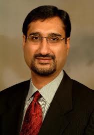
Jaswinder Ahuja, corporate vice president and MD, Cadence Design Systems, speaks to Jalaja Ramanunni and Dilin Anand of EFY.

Q. What verticals does Cadence focus on with its design automation solutions?
A. The EDA tools that we develop are in a way horizontal which means that they can be used to do designs in any of the verticals be it medical designs, defence and aerospace, industrial computations, etc. This is because the fundamental design challenges and problems across these verticals are quite similar. Where we do have certain solutions that are targeted towards certain verticals is among specific methodologies that are built on top of these designs and some IP that is targeted for the class of designs that is targeting these different verticals.
Q. What kind of challenges does each vertical bring up for the designer?
A. The nature of challenges that each vertical offers is quite different. Take consumer products, consumers are very demanding and discerning and in a sense fickle in what they will choose to buy. Thus performance, price and appearance become key considerations for their purchase decisions. This has a ripple effect on design challenges because we need to be able to design fairly advanced electronics at a very low price point. That actually requires us to use very advanced design methods and design techniques.
If you look at applications in medical electronics, this is different since here it is going to be something that is close to the human body or even embedded within the body. In the defence and aerospace sectors, you would want zero failures. Here reliability comes into play bringing up yet another different set of design challenges.
Q. What evolving trends have you observed in these EDA tools?
A. If you look at some trends in design that are common across these verticals, there are some things that are really obvious. First, power considerations are very important. Regardless of the end application, low power design or power efficient design is going to be a key. It also ties to the overall macro theme of green energy and environmental protection.
Second, if you look at further miniaturisation where we move into further advanced process nodes which is at the heart of Moore’s Law and is driving the electronics industry. Right now we are looking at 28nm as mainstream going into 20, 14, 10 and perhaps 7nm at some point. Now that is going to pose tremendous design challenges.
Given the nature of applications, and a drive towards SoC and more functionality on the chip, mixed signal design is going to become critical. Another vector is that as designs become large and complex, the verification of these designs becomes an even bigger challenge.
The next one would be the increased use of IP, having a portfolio of IP and methodologies to rapidly integrate IPs to create design. Last but not the least, at the end of the day, the end-users care about the system which has both hardware and software. Methodologies to do design allow us to conceive the product at a system-level and then make us understand what the silicon needs to be and then builds it back up again looking at hardware and software put together.
Q. What does your Indian R&D centre focus on?
A. The Indian R&D centre works on the entire portfolio of products that Cadence has to offer. Some of the products are completely led by our technical teams in India and some others are worked on together with the technical teams in other parts of the world.
Q. Could you elaborate on Cadence’s presence in India?
A. Cadence has been present in India since 1987. We have a fairly large Corporate Resource Center in Noida, with 800 odd people working out of that centre. It is mostly R&D, but there is Global IP and Global Customer support functions. We have another centre in Bengaluru where we have close to 270 odd people working on a combination of R&D, application engineering focus on end customer markets in India, services and other functions. We have another small centre in Hyderabad as well.
Q. What are your target markets in India?
A. If you look at the composition of the market, it is mostly the large MNCs who have significant design centres in India. Then there are also the design services companies, various government and defence labs in India that are doing electronics design or research in electronics design. And there are the upcoming breeds of start-up companies that are doing products or IP out of India.


