There has been more than enough talk around setting up a semiconductor manufacturing ecosystem in India but almost zero discussion on whether the small and medium sized companies can fit in or not. If these can fit in, what are the opportunities available, and what’s the best way to grab them!
“Semiconductors are a very big opportunity today. They are the key to everything electronic now. The vertical is becoming more and more important because electronics are becoming more and more intelligent. ELCINA is of view that India needs more ATMPs in the country to be able to take Fabs forward. I feel that ATMPs and OSATs will help us attract Fabs in India,” says Rajoo Goel, secretary general, ELCINA.
The government of India, has recently announced a programme for promoting semiconductor manufacturing in the country. This programme, worth over `760 billion, aims to not only provide incentives to semiconductor fabs but also to organisations present in the semiconductor design. The move seems brilliantly timed as the world is currently haunted by the shortage of semiconductors. Moreover, as the semiconductors are the brains behind modern electronics, they are of strategic value to all the countries.
“It’s a fact that the electronics industry was crushed in the early part of the millenium. The situation now, thanks to the government’s bold PLI and SPECS programme, is changing for good. India’s electronics industry has shown tremendous growth. We have seen the end product EMS come up. It has the capability of helping establish a better ecosystem of manufacturing components in the country. This is a catalytic reaction that will drive the growth of components and as well as end products in India,” shares Dr Ashwini K. Aggarwal, PhD, FIETE, Director, Applied Materials India.
Semiconductors, as a matter of fact, have been on the radar of the government of India for a long time now. The government of India has admitted that in the current geopolitical scenario, trusted sources of semiconductors and displays hold strategic importance and are key to the security of critical information infrastructure.
“Semiconductor manufacturing has been a mirage for India for the past several decades. India’s semiconductor aspirations have remained unsatiated despite the magnitude of opportunities possible. When we stand as a nation and say we will, then we will,” says Ashwini.

Opportunity in numbers
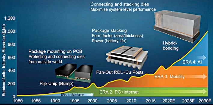
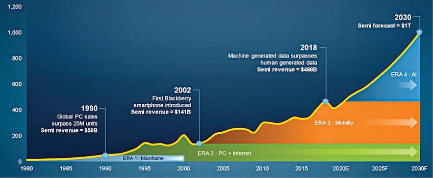
The semiconductor industry, as per Applied Materials, will be worth over $1 trillion in 2030. Industry 4.0 is being termed as one of the major factors driving this growth. As a matter of fact, machines had already surpassed the amount of data being generated by humans in the year 2018 itself. Seagate UK estimates that by 2025 there will be 175 zettabytes of data in the global datasphere. That in simple words means that the world will be generating more than 463 exabytes of data every day! Please note, the world here denotes data created by humans, machines, and the internet.
“90% of the data generated, by the end of this decade, will be by machines. Machines themselves are creating a jump in the amount of data, then humans are also driving this growth. As the amount of data generation grows, so will the need for computing. This will lead to a tremendous demand for semiconductors. I think this has been the concern of a lot of policy makers. The rate at which the demand of semiconductor is growing, it can play havoc at how national economies function,” explains Ashwini.
Our country relies 100% on imports for meeting its semiconductor needs. The value of semiconductors that India will be importing by 2025 is forecast to be around $100 billion. China, which was till recently referred to as the world’s electronics factory, imported around $378 billion worth of semiconductors during the year 2020. China currently holds 7.6% share of semiconductors sold in the world. This is another fact that makes it critical for India to establish a semiconductor manufacturing ecosystem as soon as possible.
The global semiconductor packaging market, as per Allied Market Research, is expected to reach $60.44 billion by 2030 from $27.1 billion in 2020, growing at a CAGR of 9.1% from 2021 to 2030.
“The opportunities are immense. All the stakeholders belonging to India’s electronics sector agree that this industry would hit the size of $300 billion by the year 2025. The market for semiconductors by 2030 will go to probably $1.2 trillion. India consumes about five to six percent of the total semiconductors consumed in the world. This number is going to increase, keeping in mind that we represent 18% of the world’s population,” says Amrit Manwani, MD, Sahasra Group.
The segments which are driving and will continue to drive the growth of not just the semiconductors industry but the overall components industry involve mobile phones, IT hardware, LED lighting, power electronic devices, automotive, telecom, consumer electronics, healthcare devices, and defense electronics.
OSAT before fab
Experts are divided on the best steps towards establishing a semiconductor manufacturing ecosystem in the country. Some opine that the perfect route goes through establishing fabs as the first step, some say OSATs/ATMPs should come first, while others advise on strengthening the semiconductor design ecosystem. Frankly, there are countries where the design ecosystem is stronger than fabs or OSATs, and vice versa as well.
“It will take time for the semiconductor fabs to come into the country. Before we do that downstream, we must have an ecosystem which explains what we are going to do with the wafers. Are we just going to supply these overseas? If this happens then another question will pop up in the form of why we set up the fabs in the first place if we were not able to package them here. It’s very important that we have a packaging base established in the country,” shares Manwani.
Now, while it’s not a rule, setting up an OSAT/ATMP can be achieved at least a year faster than setting up a fabrication plant. It’s also a fact that establishing an ATMP requires less investment than a fab, and also not as highly skilled professionals as a fab would require. For example, Sahasra is investing close to `1.5 billion in building an ATMP unit, while the Tata’s are rumored to be putting in more than `3.5 billion in the same. Investing in establishing a fab, in comparison, will require at least a $1 billion!
There are more than 150 companies operating in the memory packaging business in the world, though none in India, and we consume 10 to 12% of the memory chips. But then if OSATs are the right step towards enabling a semiconductor manufacturing ecosystem, why has India not been able to cash-in on this opportunity in the modern times?
“The lead time for equipment required for semiconductor packaging has gone high because of the massive semiconductor shortage worldwide. The dealers are now quoting delivery time of more than 50 days for the equipment deliveries. The prices have increased by about 15 to 20 percent. Process stability as well as keeping up with the new technology are a few more challenges. Yield is another big challenge,” explains Manwani.
“One of the reasons that we are discussing semiconductors and India is because we understand that it is a big opportunity for the nation as well as for Indian organisations. It is a huge growth area,” says Raja Manickam, CEO, Tata OSAT.
Breaking myths
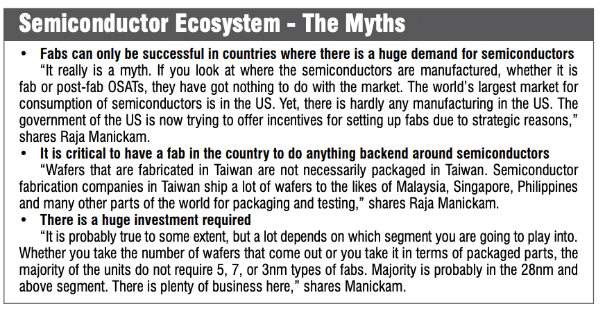
The semiconductor industry, probably the most aggressive in terms of growth, is also haunted by a number of myths, and the magnitude of these myths multiplies when countries like India attempt to establish an ecosystem. One of the most prevalent yet most unaddressed myths around the semiconductor industry starts with the fake logic that fabs can only be successful in countries where there is a huge demand for semiconductors.
“It really is a myth. If you look at where the semiconductors are manufactured, whether it is fab or post-fab OSATs, they have got nothing to do with the market. The world’s largest market for consumption of semiconductors is in the US. Yet, there is hardly any manufacturing in the US,” shares Manickam.
The majority of semiconductor fabrication, as a matter of fact, takes place in countries like Taiwan and Korea. The back-end is carried out in countries like the Philippines, Malaysia, and Singapore. In 2020, the semiconductor industry in the United States, as per Statista, accounted for 47% of the global semiconductor market. However, taking a recent Wall Street Journal report into account, Taiwan is the country that is currently producing the most number of chips in the whole world. The distance between the top consumer (United States) and the top fabricator (Taiwan) is approximately 12,333km by sea. Additionally, the local market for semiconductor consumption in Taiwan stands nowhere close to the one in the States.
“You do not need to have a local market in order to play in this business. The narrative needs to change, and we need to convey that we are going to be global suppliers. It could be a small company, medium sized company, or a large company. You could be making a small frame that could go into a test equipment. You will probably make thousands of them,” explains Manickam.
The second myth around semiconductors revolves around having a fab in the country to do anything backend around semiconductors. However, most forget that wafers are probably the most convenient to get shipped across continents.
“You can literally have millions of dyes in a box, which can fit into an individual’s hands. If you are working on a simple analogue device, you can have 20,000 to 25,000 chips from just one wafer. They are light and thin, making weight not an issue in the business,” says Manickam.
Wafers that are fabricated in Taiwan are not necessarily packaged in Taiwan.
Semiconductor fabrication companies in Taiwan ship a lot of wafers to the likes of Malaysia, Singapore, Philippines, and many other parts of the world for packaging and testing. These wafers then get assembled somewhere else.
“That’s the second myth, we do not need a fab to be in the semiconductor business,” explains Manickam.
The third myth, and probably the one that hinders most when it comes to setting up a semiconductor fabrication plant, revolves around the amount of investment required to do so. This myth, in some sense, is true. Setting up modern and up-to-date technology enabled semiconductor fabrication plants do require billions of dollars in investment. The likes of SK Hynix, TSMC, Samsung, and more announcing new fabrication plants worth billions of dollars do cement this fear, but not all the plants require the same kind of investment.
“It is probably true to some extent, but a lot depends on which segment you are going to play into. Whether you take the number of wafers that come out or you take it in terms of packaged parts, the majority of the units do not require 5, 7, or 3nm types of fabs. Majority is probably in the 28nm and above segment. There is plenty of business here,” explains Manickam.
He adds, “Those fabs are not in the $10 billion investment range. Depending on what you do, these could be in the half a billion to one billion investment bucket. Then you can have specialised fabs like Silicon Carbide fabs. These are also now becoming mainstream, whether they are Silicon Carbide or GaN. The wafers are small, the kind of circuits that go in are different and simple. They are just in the $20 to $50 million investment range. The key to right investment lies in picking the right area and building your dominance into it.”
There are thousands of small and medium companies in countries like Korea and Taiwan supporting the big names like TSMC, UMC, and ASC. A lot of these are family-run businesses. The key to their success, as Manickam shares, has been their vision to be global.
“The test tools that are required for testing semiconductors once they are packaged are more or less designed in India. But as these belong to multinational companies, they are taken away and sold at 10x the price. If we had that capability here in the country, it will go a long way,” adds Manwani.

SMEs as India’s strengths
While there are no brownie points for guessing that India missed the semiconductor boat a long time ago, there is definitely a whole cake waiting to be devoured for individuals and organisations who understand that the changing geo-political conditions have led us towards a new boat full of opportunities. However, following the same business model as other semiconductor OSAT and fabs might not work for India.
“We have some strengths in India. One of them is engineering, we are innovative, and we can scale the engineering as well. We can do a lot of customised work. If you look at all the other countries that are operating in the OSAT space, you will find that they have access to capital. They talk about 2 to 3 percent (interest on loan) whereas in India we talk about 10 to 12 percent. Cost of capital is very high for us,” shares Manickam.
He adds, “They are who they are because they didn’t have the kind of breadth of engineering or the scalability in engineering. They ended up investing more and more capital in order to survive. Business is only two things, it is capital and it is labour. In our case we have talented labour. However, we never put too much stress in capital because we were able to create the world’s IT industry here in India. The other countries did not have such talented labour and hence they had no choice but to put in a lot of investment.”
China is the biggest example of what can happen when you put in a lot of capital. The country, some decades back, lacked quality manpower and hence it grew by investing capital. Semiconductors dot Org forecasts that the Chinese will be investing anything around $12 to $15 billion. Thanks to the government of China the country has announced over 110 fab projects since the year 2014. The investments in these fabs are around $196 billion.
“The good they did was they did not allow the foreign companies to come in and dominate. They had home-grown companies. That is why there is no Google and Facebook in China.
They never hesitated in putting barriers on the chip-side too. China, in terms of chips, probably has every catalogue product being done by someone in China. There are hundreds of companies like that and then there are hundreds of fabs who can support these companies,” shares Raja Manickam.
Why China has been so successful in the same, as Manickam answers, is because companies there do not want to do everything. One company focuses on one thing, which could be design, support, or fabrication. The semiconductor industry has many segments where the small and medium sized companies can help. Equipment required for semiconductors is also a big segment.
“At the same time there are things that SMEs can make for the big instrument making brands. If we can incentivise big names like Intel and TSMC, we can also ask them what they can do for the SMEs to prosper and add new things to their product range. We might want to be more savvy about the PLI schemes and ask the benefitters what are they giving us back apart from jobs,” shares Manickam.

The opportunity(ies)
The semiconductor ecosystem is not just about designing, fabricating, or packaging semiconductors. It is actually a Pandora’s box of opportunities for small and medium companies. The opportunity to supply raw materials, the opportunity for making software, the opportunity for transporting chips, and more. The biggest of these opportunities lies in working consistently to create dominance in what a company, whether small or big, does around semiconductors.
“There is a big number of small companies playing in this arena. They are supplying chemicals, raw materials, products like valves, and much more to the ecosystem. There is whole bunch of requirements. Small and medium companies need to pick where their strength lies. For example, if a founder has a major in chemistry, there is enough room for working around the chemistry used in the field of semiconductors,” shares Manickam.
Applied Materials has recently applied to the Central government and the government of Karnataka to be an anchor account that can create ancillaries for its procurement requirements. The company, on an average, buys $3 billion worth of specialised equipment and parts from Asia Pacific region. The company has expressed that India can supply materials to it worth over `10 to 20 billion annually.
“We have discovered gems in India during this process. These belong to the verticals of specialised assembly components, and some of these are also SPECS applicants. There will also be a supply chain for equipment that we will generate out of India,” says Ashwini.
The fact that there are a lot of Indians working in the semiconductor ecosystem outside India can also prove to be one of the biggest strengths for the country. When Morris Chen, the founder of TSMC, started working in the semiconductor fab business, there were only a handful of Taiwanese nationals in the vertical. There are a lot more Indians working in the semiconductor ecosystem than what was the scene for Taiwan in the 1980’s.
“People like me went outside India in the 1970’s and 80’s. A lot of us still carry the baggage of what India was like at that time. Now there’s a lot more pull to bring in stuff and technology than the push,” says Manickam.
Mukul Yudhveer Singh is a Business Editor at EFY


