


Heterogeneous computing refers to systems which use more than one kind of processor or cores to maximise performance or energy efficiency. The processors incorporate specialised processing capabilities to handle particular tasks.
Heterogeneous architectures break away from the traditional evolutionary processor design path, posing new challenges and opportunities in high-performance computing.
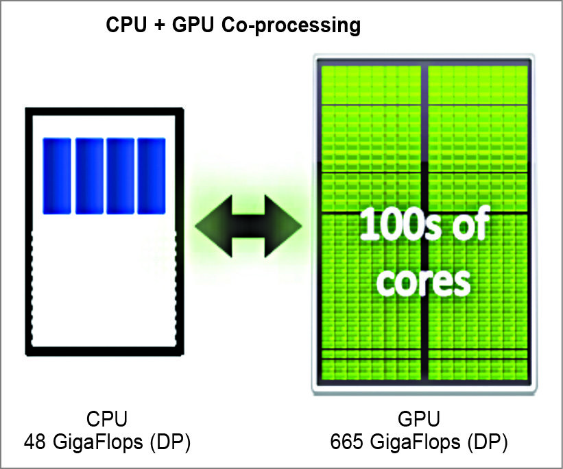
Heterogeneous computing will continue to add many cores and hardware features such as transactional memory, random number generators, scatter/gather and wider single-instruction multiple-data/advanced vector extensions, ensuring synergies with big data, mobile and graphics markets. It has the potential to achieve greater energy efficiency by combining traditional processors with unconventional cores such as custom logic, field-programmable gate arrays (FPGAs) or general-purpose graphics processing units (GPUs). Instead of using just a single CPU or GPU, heterogeneous architectures add an application-specific integrated circuit (ASIC) or FPGA to perform highly dedicated processing tasks. Heterogeneous architectures achieve performance gain by parallelism instead of clock frequency.

Parallelism
There are four levels of parallelism in hardware: single-instruction single-data (SISD), single-instruction multiple-data (SIMD), multiple-instruction single-data (MISD) and multiple-instruction multiple-data (MIMD).
SISD.
In SISD, there are tens to hundreds of data paths, which all run by one instruction stream. General-purpose host CPU executes the main application, with data transfer and calls to the SIMD processor for compute-intensive kernels. SIMD has dominated high-performance computing (HPC) since the time of Cray-1 supercomputer.

SIMD.
SIMD performance depends on hiding random-access memory latency, which may be hundreds of cycles, by accessing data in big chunks at a very high memory bandwidth. Data-parallel feed-forward applications are common in HPC. Large register files are provided in data paths to hold large regular data structures such as vectors.
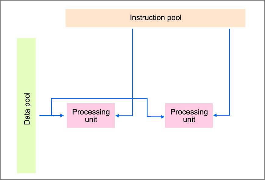
MISD.
It is a type of parallel computing architecture where many functional units perform different operations on the same data. Pipeline architectures belong to this type, though a purist might say that the data is different after processing by each stage in the pipeline. There is a sequence of data transmitted to the set of processors. Each processor executes a different instruction sequence.
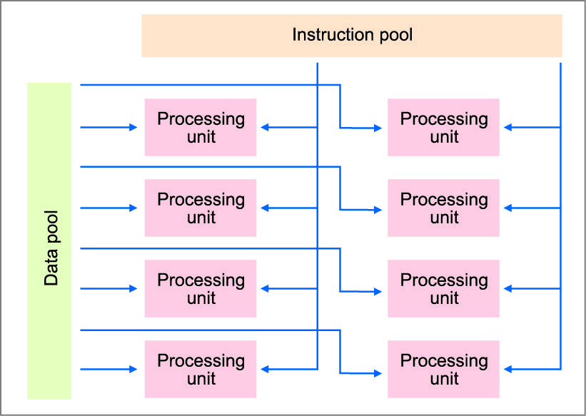
MIMD.
MIMD class of parallel architecture is the most familiar and possibly most basic form of parallel processor. MIMD architecture consists of a collection of ‘n’ independent, tightly-coupled processors, each with a memory that may be common to all processors, and/or local and not directly accessible by the other processors.
Two subdivisions of MIMD are single-program multiple-data (SPMD) and multiple-program multiple-data (MPMD). Single-chip cell broadband engine architecture consists of a traditional CPU core and eight SIMD accelerator cores. It is a very flexible architecture, where each core can run separate programs in MPMD fashion and communicate through a fast on-chip bus. Its main design criteria has been to maximise performance whilst consuming minimal power. It defines a new processor structure based upon the 64-bit Power Architecture technology, but with unique features directed toward distributed processing and media-rich applications.
The cell broadband engine architecture defines a single-chip multiprocessor consisting of one or more power processor elements (PPEs) and multiple high-performance SIMD synergistic processor elements (SPEs). For example, a GPU with 30 highly multi-threaded SIMD accelerator cores in combination with a standard multicore CPU.
The GPU has a vastly superior bandwidth and computational performance, and is optimised for rerunning SPMD programs with little or no synchronisation. It is designed for high-performance graphics, where data throughput is the key. FPGA scan also incorporates regular CPU cores on-chip, making it a heterogeneous chip by itself. FPGAs can be viewed as user-defined ASICs that are reconfigurable. These offer fully deterministic performance and are designed for high throughput, for example, in telecommunication applications.
Accelerator cores are designed to maximise performance, given a fixed power or transistor budget. These use fewer transistors and run at lower frequencies than traditional CPUs.
Algorithms such as finite-state machines and other intrinsically serial algorithms are most suitable for single-core CPUs running at high frequencies. Parallel algorithms such as Monte Carlo simulations, on the other hand, benefit greatly from many accelerator cores running at a lower frequency. Most applications consist of a mixture of such serial and parallel tasks, and ultimately perform best on heterogeneous architectures.
Mobile heterogeneous computing
Mobile systems are more intelligent than ever. As users demand more functionality, designers are continually adding to a growing list of embedded sensors. Image sensors support functions such as gesture and facial recognition, eye tracking, and proximity, depth and movement perception. Health sensors monitor the user’s EKG, EEG, EMG and temperature. Audio sensors add voice recognition, phrase detection and location-sensing services.
Consequently, major silicon vendors now spend their transistor budget on symmetric multi-core processors for the mass market. This evolutionary path might suffice for two, four and perhaps eight cores, as users might run that many programs simultaneously. However, in the foreseeable future we will most likely get hundreds of cores. This is a major issue: If silicon vendors and application developers cannot give better performance to users with new hardware, the whole hardware and software market will go from selling new products to simply maintaining existing product lines.
Today’s multi-core CPUs spend most of their transistors on logic and cache, with a lot of power spent on non-computational units. Processor design has always been a rapidly evolving research field. Many of these same devices now offer ‘context-aware’ subsystems that allow the system to initiate highly advanced, task-enhancing decisions without prompting the user. For example, temperature, chemical, infrared and pressure sensors can evaluate safety risks and track a user’s health in dangerous environments. Precision image sensors and ambient light sensors can boost image resolution and display readability automatically as environmental conditions change.
These new capabilities significantly impact system design. To optimise decision-making, these devices must collect, transfer and analyse data as quickly as possible. The faster the system responds, the more accurately it can adapt to rapidly changing conditions. Furthermore, since ‘context-aware’ systems must be ‘always on’ to track changes in the environment, these new capabilities significantly drain system power.
To address this problem, a growing number of developers are adopting mobile heterogeneous computing (MHC) architectures. One of the primary reasons why system designers are moving to MHC is the ability it gives developers to move repetitive computation tasks to the most efficient processing resources so as to lower power consumption. For example, one key distinction between GPUs, CPUs and FPGAs is how they process data. GPUs and CPUs typically operate in a serial fashion, performing one calculation after another.

Designers’ approach
If designers want to reduce system latency to respond to sensor inputs in real time, they must accelerate the system clock and, in the process, increase power consumption. FPGAs, on the other hand, enable a system to perform calculations in parallel, which, in turn, reduces power consumption, particularly in compute-intensive repetitive applications.
The fact that FPGAs have thus far been used sparingly for these tasks can be attributed to a common misconception—many designers think of FPGAs as relatively large devices. However, this is not necessarily the case. Low-density FPGAs offer a number of other advantages in the current generation of intelligent systems.
The rapid proliferation of sensors and displays in today’s mobile devices presents new challenges from an input/output (I/O) interface perspective. Designers must integrate sensors and displays with a growing diversity of interfaces, including legacy systems using proprietary or custom solutions.
In many cases, designers can use low-density FPGAs or programmable application-specific standard products built around an FPGA fabric to aggregate data from multiple sensors onto a single bus or bridge between multiple disparate interfaces. With reprogrammable I/Os, these FPGAs are capable of supporting a wide variety of bridging, buffering and display applications. The recent emergence and rapid adoption of low-cost Mobile Industry Processor Interfaces (MIPI) such as CSI-2 and DSI has helped to simplify this task. By utilising the latest advances in I/O from the mobile computing market and MIPI together with the inherent advantages of low-density programmable logic in MHC architectures, designers can optimise their systems’ ability to collect, transfer and analyse this key resource.
CUDA approach
CUDA architecture enables general-purpose computing on the GPU and retains traditional DirectX/OpenGL graphics. The dominance of multi-core systems in all domains of computing has opened the door to heterogeneous multi-processors. Processors of different compute characteristics can be combined to effectively boost the performance per watt of different application kernels.
GPUs and FPGAs are becoming popular in PC-based heterogeneous systems for speeding up compute-intensive kernels of scientific, imaging and simulation applications. GPUs can execute hundreds of concurrent threads, while FPGAs provide customised concurrency for highly parallel kernels. However, exploiting the parallelism available in these applications is currently not a push-button task. Often the programmer has to expose the application’s fine and coarse grained parallelism by using special application programming interfaces (APIs).

OpenMP
OpenMP (Open Multi-Processing) API supports multi-platform shared memory multiprocessing programming in C, C++ and Fortran. It consists of a set of compiler directives, library routines and environment variables that influence run-time behaviour.
OpenACC
OpenACC (for open accelerators) is a programming standard for parallel computing developed by Cray, CAPS, Nvidia and PGI. The standard is designed to simplify parallel programming of heterogeneous CPU/GPU systems. The programmer can annotate C, C++ and Fortran source code to identify areas that should be accelerated using compiler directives and additional functions.
The four steps to accelerate the code include: Identify parallelism, express parallelism, express data locality and optimise.
Selection of CUDA
The selection of CUDA as the programming interface for FPGA programming flow offers three main advantages:
1. It provides a high-level API for expressing coarse grained parallelism in a concise fashion within application kernels that are going to be executed on a massively parallel acceleration device.
2. It bridges the programmability gap between homogeneous and heterogeneous platforms by providing a common programming model for clusters with nodes that include GPUs and FPGAs. This simplifies application development and enables efficient evaluation of alternative kernel mappings onto the heterogeneous acceleration devices without time-consuming kernel code rewriting.
3. Wide adoption of the CUDA programming model and its popularity render a large number of existing applications available to FPGA acceleration.
Even though CUDA is driven by the GPU computing domain, CUDA kernels can indeed be translated with FCUDA into efficient, customised multi-core compute engines on the FPGA.
CUDA programming
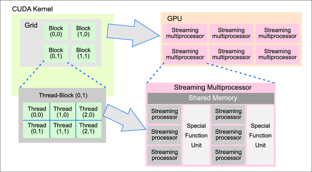
CUDA enables general-purpose computing on the GPU (GPGPU) through a C-like API which is gaining considerable popularity. The CUDA programming model exposes parallelism through a data-parallel SPMD kernel function. Each kernel implicitly describes multiple CUDA threads that are organised in groups called thread-blocks. Thread-blocks are further organised into a grid structure (Fig. 6).
Threads within a thread block are executed by the streaming processors of a single GPU streaming multiprocessor and allowed to synchronise and share data through the streaming multiprocessor’s shared memory. On the other hand, synchronisation of thread-blocks is not supported.
Thread-block threads are launched in SIMD bundles called ‘warps.’ Warps consisting of threads with highly diverse control flow result in low performance execution. Thus, for successful GPU acceleration it is critical that threads are organised in warps based on their control flow characteristics.
The CUDA memory model leverages separate memory spaces with diverse characteristics. Shared memory refers to on-chip SRAM blocks, with each block being accessible by a single streaming multiprocessor (Fig. 6). Global memory, on the other hand, is the off-chip DRAM that is accessible by all streaming multiprocessors. Shared memory is fast but small, whereas global memory is long-latency but abundant. There are also two read-only off-chip memory spaces, constant and texture, which are cached and provide special features for kernels executed on the GPU.
FASTCUDA
FASTCUDA platform provides the necessary software toolset, hardware architecture and design methodology to efficiently adapt the CUDA approach into a new FPGA design flow. With FASTCUDA, CUDA kernels of a CUDA-based application are partitioned into two groups with minimal user intervention: those that are compiled and executed in parallel software, and those that are synthesised and implemented in hardware. An advanced low-power FPGA can provide the processing power (via numerous embedded micro-CPUs) and logic capacity for both software and hardware implementations of CUDA kernels.
FASTCUDA approach
Today’s complex systems employ both software and hardware implementations of components. General-purpose CPUs, or more specialised processors such as GPUs, running the software components, will routinely interact with special-purpose ASICs or FPGAs that implement time-critical functions in hardware. In these systems, separation of duties between software and hardware is usually very clear. FASTCUDA aims to bring software and hardware closer together, interacting and cooperating for execution of a common source code. As a proof of concept, FASTCUDA focuses on source codes written in CUDA.
Source code example follows:
[stextbox id=”grey”]
//kernel
__global__ void vectorAdd (float *A, float *B, float *C) {
int i = threadIdx.x;
C[i] = A[i] + B[i];
}
# define N 100
#define M N*sizeof (int)
//host program
main() {
int A[N], B[N], C[N];
…
//copy input vectors from host memory to device memory
cudaMemcpy( d_A, A, M, cudaMemcpyHostToDevice);
cudaMemcpy( d_B, B, M, cudaMemcpyHostToDevice);
// kernel invocation
vectorAdd<<<1,N>>>(d_A, d_B, d_C);
//copy output vectors from device memory to host memory
cudaMemcpy(C, d_C, M,
cudaMemcpyDeviceToHost );
…
}
[/stextbox]
Threads within a thread-block are synchronised, and executed by a single streaming multiprocessor inside a GPU. These share data through a fast and small private memory of the streaming multiprocessor, called ‘shared memory.’ On the other hand, synchronisation between threads belonging to different thread-blocks is not supported. However, a slow and large ‘global memory’ is accessible by all thread-blocks.
Similar to a GPU, FASTCUDA employs two separate memory spaces (global and local) as well as a similar mapping of the block-threads onto the FPGA resources. Bringing software and hardware close together, FASTCUDA accelerates execution of CUDA programs by running some of the kernels in hardware. A state-of-the-art FPGA will provide all the required resources; multiple embedded micro-CPUs for the host program and software kernels, and logic capacity for hardware kernels.
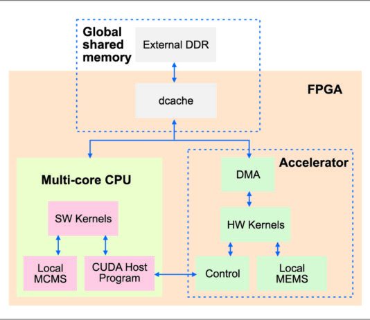
Fig. 7 shows the block diagram of the overall FASTCUDA system. A multi-core processor, consisting of multiple embedded cores (configurable small processors), is used to run the host program serially and software kernels in parallel. Threads belonging to the same CUDA thread-block are executed by the same core. Hardware kernels are partitioned into thread-blocks, and synthesised and implemented inside an ‘accelerator’ block. Each thread-block has a local private memory, while the global shared memory can be accessed by any thread following the philosophy of the CUDA model.
The FASTCUDA toolset (Fig. 8) is responsible for automating most of this process, thus minimising user intervention.

Design space exploration
The first step is to decide how to make the best use of the available FPGA resources for a given CUDA program. The next is to know what percentage of the FPGA real estate should be allocated to the multi-core processor for software kernels, and what percentage should be allocated to the accelerator for hardware kernels. This is followed by the information on which kernels are to be run in software and which in hardware, area-speed tradeoff best for each of the harware kernels and optimal configuration (number of cores, cache sizes, memory banks, etc) for the multi-core processor. This is done by carefully examining through several simulation and synthesis runs.
The simulation tool provides runtime estimates for execution of each kernel in software, for several configurations of the multi-core processor (with varying cache sizes, memory banks, etc). The synthesis tool provides latency estimates for execution of each kernel in hardware, with varying hardware footprints (trading area for speed).The design space exploration tool uses these area and performance estimates, along with its full knowledge of the underlying platform’s resources and available configurations, to heuristically search for the best answers to the questions listed above. User experience can be used to guide the tool, e.g., by restricting the search to a smaller set with the most ‘interesting’ multi-core configurations.
Multi-core processor
The CUDA host program as well as software kernels, i.e., the subset of kernels determined by the design space exploration tool, run in software on the multi-core processor (Fig. 9).
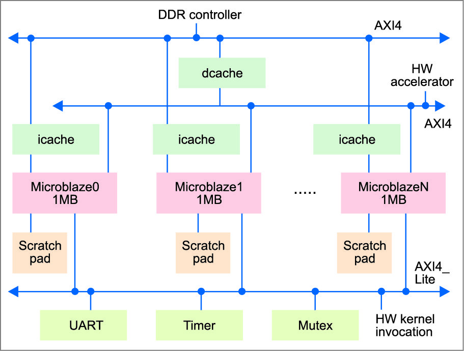
It uses Xilinx Microblaze soft cores with separate instruction caches and a shared data cache, all communicating through two AXI4-based buses. FASTCUDA follows a similar mapping of the threads with a GPU. Each core executes thread-block, which can use the core’s scratchpad memory as a private local memory. All the threads from any thread block can access the global shared memory, which can also be accessed by the hardware accelerator. The AXI4_Lite bus is used for communication between the multi-core processor and the accelerator block that is running hardware kernels. A simple handshake protocol is employed to pass the arguments and trigger a specific hardware kernel to start running, which will then respond back when it has finished running. Lastly, the timer and mutex blocks on the AXI4_Litebus are a requirement for symmetric multiprocessing support of the runtime on the processor.
Implementing CUDA kernels on the multi-processor
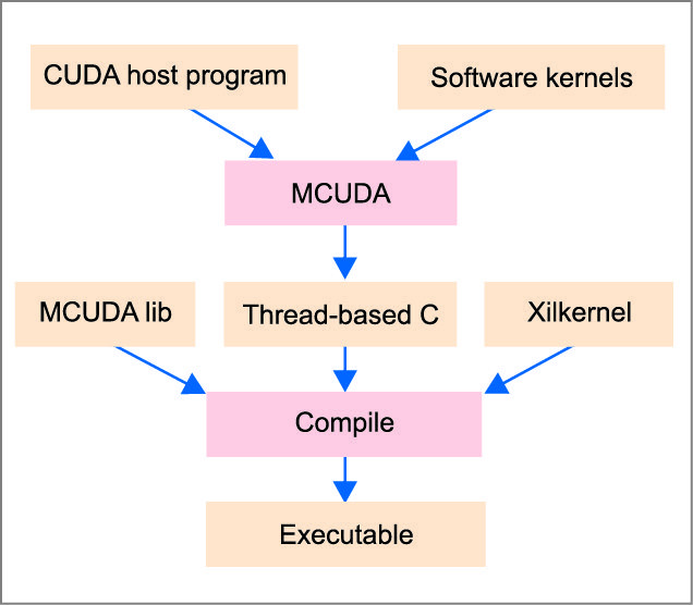
The OS-level software running on the multi-core processor here is a modified version of the Xilinx kernel ‘Xilkernel.’ Xilkernel supports POSIX threads, mutexes and semaphores, but was meant to run on a single core, thus having no support for an SMP environment like the one here. We consequently had to add SMP support to Xilkernel. CUDA kernels are supposed to run on SIMT devices (GPUs), which are drastically different from multi-core processors. Thus, the next step is to port the CUDA kernels, using MCUDA, to run on top of the multi-core multi-threaded environment provided by modified Xilkernel.
MCUDA transforms the CUDA code into a thread-based C code that uses MCUDA library in order to create a pool of threads and coordinate thread operations as well as provide the basic CUDA runtime functionality for kernel invocation and data movements. Xilkernel provides the mutex support required by MCUDA library and the thread-based support required by multi-threaded software kernels. In CUDA the host program is usually run on a chip separate from the CUDA kernels; the first is run on a general-purpose CPU and the latter on a GPU. Thus the CUDA programming model assumes that the host and device maintain their own separate memory spaces, referred to as host memory and device memory, respectively.
The execution of a kernel involves:
1. Memory transfers of input vectors from the host memory to the device memory,
2. Kernel execution, which uses input vectors in order to generate output vectors and
3. Memory transfers of output vectors from the device memory to the host memory.
Addresses of input and output vectors are passed as arguments to the CUDA kernel. In contrast, FASTCUDA runs everything on the same chip, thus favouring a different memory model where all the threads of a kernel and the host program can share a single global memory. In this model, hardware kernels inside the accelerator have direct access to the memory in order to read their input vectors and write output vectors.
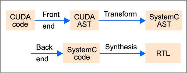
Implementing CUDA kernels in hardware
In FASTCUDA, the code of hardware kernels is preprocessed before synthesis. To aid in this preprocessing the programmer is required to use ‘#pragma’ directives in order to specify which ones among the kernel arguments are inputs and outputs, as well as their sizes. The result of translation from CUDA to SystemC is given below:
[stextbox id=”grey”]//SystemC module\
SC_MODULE (addMod) {
sc_in A, B, C, threadIdx_x;
sc_port sMem, gMem;
sc_in clk, start;
sc_out done;
SC_CTOR(addMod) {
SC_CTHREAD(add, clk);
reset_signal_is(start);
}
// kernel
void add() {
int i = threadIdx_x;
gMem.writeFloat (C+i,
gMem.readFloat(A+i) +
gMem.readFloat(B+i));
}
[/stextbox]
SystemC interface called ‘fcMem’ is provided, like in latest GPUs, to better exploit the AXI interface bandwidth.
Potential applications
Heterogeneous systems use advances in computing architectures to deliver improvements in power efficiency, performance, programmability and portability across computing devices. However, with heterogeneous architectures, care is required by the programmer to fully utilise hardware. Potential applications include smartphones, wearables, drones, high-end cameras, human-machine interfaces, industrial automation platforms, and security and surveillance products. The architecture has the potential to accelerate design of mobile and IoT edge devices, as it can easily handle features like voice, gesture and image recognition, haptics, graphics acceleration and signal aggregation.