Gate level simulation is used to boost the confidence regarding implementation of a design and can help verify dynamic circuit behaviour, which cannot be verified accurately by static methods. It is a significant step in the verification process.
Gate level simulation overcomes the limitations of static-timing analysis and is increasing being used due to low power issues, complex timing checks at 40nm and below, design for test (DFT) insertion at gate level and low power considerations. For DFT, scan chains are inserted after the gate-level netlist is created; gate level simulation is often used to determine whether scan chains are correct.
Technology libraries at 45nm and below have far more timing checks and complex timing checks than older process nodes. Gate level simulation may take up to one-third of the simulation time and could potentially take most of the debugging time. It is run after RTL code is simulated and synthesized into a gate-level netlist. It requires a complete reset of the design.

Reasons for running gate level simulation are reset verification, X optimism in RTL, timing verification on multi-cycle/asynchronous paths and basic heartbeat test.
In reset verification, gate level simulation can verify system initialization and show that the reset sequence is correct.

In X optimism in RTL, an RTL simulator may optimistically assign zero or one to a value that a gate level simulation would identify as X (unknown).
In timing verification on multi-cycle/asynchronous paths, static-timing analysis cannot identify asynchronous interfaces, and has constraint requirements that impact false and multi-cycle paths.
In the basic heartbeat test, some verification teams may want to run a limited sanity check to verify the functionality at the gate level. As gate level simulation runs much more slowly than an RTL simulation, it potentially has significant impact on the verification closure cycle.
Cadence incisive enterprise simulator has several features such as zero-delay simulation, built-in delay mode control functions to reduce simulation time, selectively disabling delays in sections of the model where timing is not currently a concern, detecting potential zero-delay gate loops, correcting race conditions that occur in zero-delay mode, disabling timing checks for the entire simulation or for selected blocks, controlling the number of timing check violations, using multi-snapshot incremental elaboration to improve elaboration performance, using wave dumping only if required, avoid or use selectively command-line options that provide additional information and access to objects for debugging.
Incisive also offers a timing file that lets you turn off the timing for particular instances in a design. Palladium XP accelerator/emulator can offer speeds 10,000 times faster than simulation. If full debug access is needed, a switch can provide it. There is also an option (-ZLIB) that can compress snapshots and save disk space, while letting users set the level of compression.
Running a gate level simulation
The use of static tools to reduce gate level simulation time should be used before running zero-delay information, especially for linting. Static-timing analysis can provide information that is used to start gate level simulation early in the flow.
There are many reasons for running gate level simulation, some of which are given below:
1. To give confidence in verification of low-power structures, absent in RTL and added during synthesis. It is a probable method to catch multi-cycle paths if tests exercising these are available. Power estimation is done on the netlist for power numbers
2. To verify the power-up and reset operation of the design and to check if the design has any unintentional dependencies on initial conditions
3. To verify DFT structures absent in RTL and added during or after synthesis. Scan chains are generally inserted after the gate-level netlist has been created. Hence, gate level simulation is often used to determine whether scan chains are correct. It is also required to simulate ATPG patterns. Tester pattern simulations are done on the gate-level netlist
4. To help reveal glitches on edge-sensitive signals due to combination logic; using both worst- and best-case timing may be necessary
5. To check special logic circuits and design topology that may include feedback and/or initial state considerations or circuit tricks
6. To check if design works at the desired frequency with actual delays in place. It is a probable method to find out the need for synchronisers, if absent in design. It will cause X propagation on timing violation on that flop
Gate level simulation execution strategy
In highly integrated products, it is not possible to run gate simulation for all system on chip (SoC) tests due to the simulation and debug time required. Therefore the vectors that are to be run in gate level simulation have to be selected judiciously.
Possible candidates for such vectors are test cases involving initialisation and boot up, and all blocks of the design must have at least one test case for gate level simulation, test cases checking clock source switching, cases checking clock frequency scaling, asynchronous paths in design, test cases that check entry/exit from different modes of design and dedicated tests for timing exceptions in the STA.
Gate level simulation targets the maximum desired operating frequency of the design. Some signals that are critical for gate level simulation debug can be preserved during synthesis. A list of all synchroniser flops is generated using CDC tools.
Asynchronous paths where timing checks need to be turned off are analysed and a complete list of such flops is prepared, which also includes reset synchronisers. Timing checks are turned off on all such flops to avoid any redundant debugging, otherwise these will cause X corruption in gate level simulation.
This work should ideally be done before the SDF arrives. It may happen that the names of the synchronisers in RTL and the netlist are different. All such flops should be updated as per the netlist. Also, correct standard cell libraries, correct models of analogue blocks and more should be picked for gate level simulation.
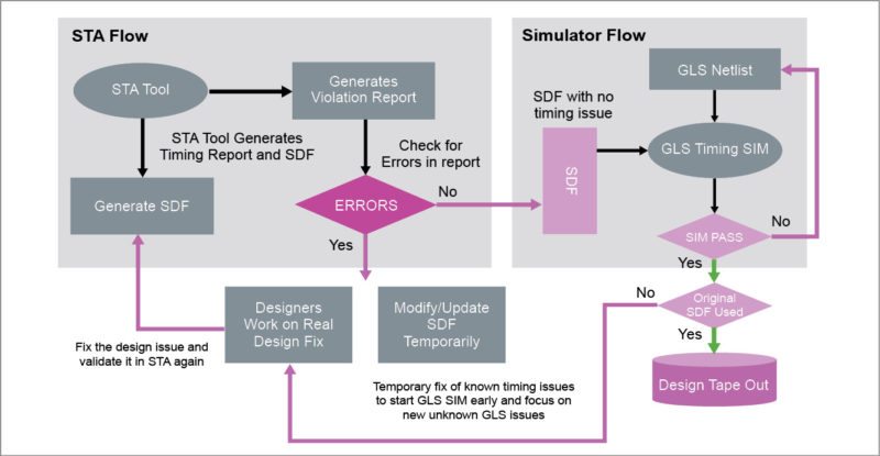
Unit-delay gate level simulation for test bench cleanup setup is done for unit delay gate level simulation and test cases that are planned to be run on gate level are run with this setup to clean the test bench. This is done because unit-delay simulations are relatively faster and all test bench/testcase-related issues can be resolved.
Running unit-delay gate level simulation is recommended because one can catch most of the test bench/testcase issues before the arrival of SDF. After SDF arrives, focus should be more on finding the real design/timing issues. So one must make sure that the time does not get wasted in debugging test-case-related issues at that time.
Challenges
The challenge in gate level simulation is X propagation debug. X corruption may be caused by a number of reasons such as timing violations, uninitialised memory and non-resettable flops. There generally are uninitialised flops in design which due to the architecture are guaranteed not to cause any problems. There is a need to find out all such flops in the design and initialise these to some random value (either zero or one) so as to mimic silicon. It gives a clear picture of how the design will behave at the desired frequency with actual delays in place.
Although gate level simulation has its own set of challenges like set-up issues and long run time, among others, it is still very much a part of the sign-off process.
V.P. Sampath is an active member of IEEE and Institution of Engineers India Ltd. He is a regular contributor to national newspapers, IEEE-MAS section, and has published international papers in VLSI and networks