


Designing a single-stage transistor amplifier requires numerous formulas to calculate various parameters, such as the values of resistors, coupling and bypass capacitors, power consumption, and current flow through different components. A good amount of time is required to calculate such parameters even with a regular calculator. Using C++ program, all the parameters can be calculated in a fraction of a second.
To design an electronic circuit like a power supply, an amplifier, oscillator or operational amplifier, certain formulae are required so that correct values of components are obtained for the intended application. Some circuits require only one formula, while others may require two or more.
The single stage transistor amplifier presented here requires a total of 19 formulae to obtain the values of components and analyse the circuit.

Table of Contents
Single stage transistor amplifier
The single stage transistor amplifier consists of a single npn transistor T1 (BC547), four resistors R1, R2, Rc and Re, two coupling capacitors C1 and C2, one bypass capacitor Ce connected across emitter resistor Re as shown in Fig. 1.
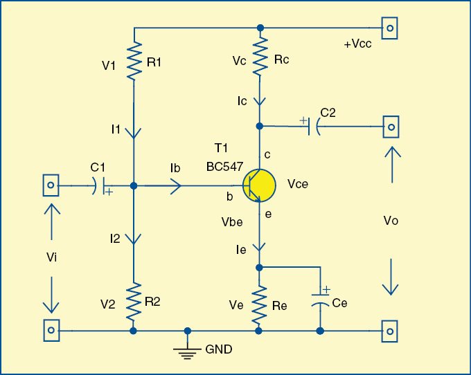
+Vcc is the supply voltage, Vi the input signal and Vo the output signal. I1, I2, Ic and Ie, as shown in the figure, are DC currents. Resistors R1, R2 and Re are used to provide proper voltages to base b, emitter e and collector c of T1, so that base-emitter junction is forward-biased and base-collector junction is reverse-biased.

Collector resistor Rc is used as the load that provides output voltage Vo. Bypass capacitor Ce is used to bypass the AC audio-frequency signal towards the ground so that constant DC emitter voltage Ve is mainained to prevent negative feedback in the amplifier. Coupling capacitors C1 and C2 are used to block the DC signal and pass the AC signal.
Design Guidelines
In order to bias the transistor properly with voltage-divider bias method, operating point Q should be at the centre of the DC load line (not shown here), where Vce= Vcc/2 and collector current Ic is as per the data sheet of the transistor. With no AC input signal, stable operating Q is maintained by using the one-tenth rule, which makes emitter voltage one-tenth of the supply voltage, Vcc. Therefore emitter voltage in volts is given by:
Ve = 0.1 Vcc
If voltage across the collector and emitter is Vce = 0.5Vcc, the remaining voltage of 0.4Vcc appears across the collector resistance.
Therefore collector resistance in kilo-ohms is given by:
 Rc = 4 x Re
 where Re is the emitter resistance.
 Base current in milliamperes is given by:
 Ib = Ic / b
where Ic is the collector current and b is the current gain of the transistor. (It is normally represented by β or h-parameter hFE).
 Therefore emitter current in milliamperes is given by:
 Ie = Ic +Ib
 Emitter resistance of the transistor in kilo-ohms is given by:
 Re = Ve/Ie
 Applying 10:1 rule of the firm voltage divider, second base resistance in kilo-ohms is given by:
 R2 =0.1 x b x Re
 The base voltage or voltage across R2 in volts is given by:
 V2 = Ve + Vbe
 where Vbe is the voltage across the base and emitter.
For the silicon transistor, Vbe = 0.7 volts. In this case, the silicon transistor is considered. Voltage across first base resistance R1 in volts is given by:
 V1 = Vcc – V2
 Therefore first base resistance in kilo-ohms is given by:
 R1 = (V1/V2) x R2
 Power consumed by the circuit in milliwatts is given by:
 P = Ic x Vcc
 Collector voltage of the transistor in volts is given by:
 Vc = Ic x Rc
 Voltage across the collector and emitter of the transistor in volts is given by:
 Vce = Vcc –(Vc + Ve)
 Current flowing through resistor R1 in milliamperes is given by:
 I1 = V1 / R1
 Current flowing through resistor R2 in milliamperes is given by:
 I2 = V2 / R2
 Power dissipated across resistor R1 in milliwatts is given by:
 PR1 = I1 x I1 x R1
 Power dissipated across resistor R2 in milliwatts is given by:
 PR2 = I2 x I2 x R2
 Power dissipated across collector resistor Rc in milliwatts is given by:
 PRc = Ic x Ic x Rc
 Power dissipated across emitter resistor Re in milliwatts is given by:
 PRe = Ie x Ie x Re
Coupling capacitors C1 and C2 and bypass capacitor Ce in micro-farads is given by:
C = C1 = C2 = Ce = (1000000) / ( 2 x 3.14 x f x Xc)
where f is the minimum frequency in hertz to be amplified by the transistor amplifier and Xc is the reactance of capacitors C1, C2 and Ce.
Reactances of these three capacitors are considered to be the same, which is 1000 ohms.
Software Program
All 19 formulae mentioned above are programmed using C++ language. The circuit has been tested using Turbo C++ version 3 and Visual C++ IDE on Windows 7.
Download source code: click here
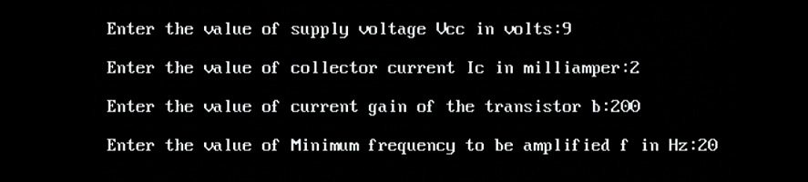
After running the program, it prompts you to enter the values of DC supply voltage Vcc, bias collector current of transistor Ic, current gain of transistor b and minimum frequency f to be amplified by the transistor amplifier.
For example, enter Vcc = 9, Ic = 2, b = 200 and f = 20 as shown in Fig. 2.
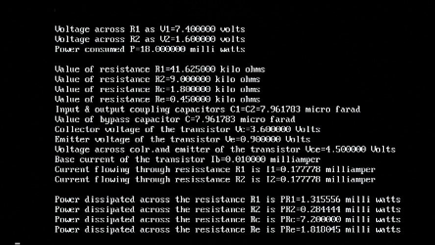
Next, hit Enter. Within a fraction of a second, all 19 parameters for the transistor amplifier are calculated and displayed on the monitor as shown in Fig. 3.
It is found that, to calculate the above 19 parameters, around 12 minutes are required. Therefore in order to save time, such a program can be quite useful for a circuit designer.
This article was originally published in January 2016 and updated in November 2024.

Thank you very much for your efforts in sharing your knowledge. I want to know if this design can be applied to the RF stage of an amplifier. I am currently building an FM power amplifier stage of an FM transmitter. if this design is not suitable for an RF power amplifier can you please help me with a design. it is a one-watt transmitter. thank you.
superrrrr excellent mind bolwing
Please I need the code
Hi Sandra, the source code is present on the second page of the article.
I’m not able to download the source code
Please help me out.
Hi Nikhil, kindly refresh the page and retry.
Please i want the full pdf document
Its very helpful and useful
Hi Justice, you can find this project in EFY Aug 2015 issue. You can also save this page as PDF on your PC.