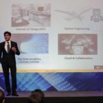
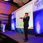
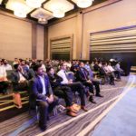
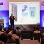
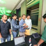
The ANSYS Electronics Simulation Expo was conducted in Bangalore on the 3rd of June 2016, with a focus on helping the engineering community improve electronic system design.
The event started off with a welcome note by Rafiq Somani, the country manager for India, ASEAN and ANZ at ANSYS. This was followed with a keynote talk delivered by Sudhir Sharma, global industry director, High Tech, ANSYS.
One of the most interesting sessions at the event was a panel discussion on “Engineering the Internet of Things”. The topic is quite apt, as most other IoT related events tend to focus only on business aspects pertaining to how massive connectivity and big data affected systems and processes.
The panel consisted of Guruprasad Mudlapur (Vice President, Robert Bosch), Apu Sivadas (Co-Founder, Steradian Semiconductors), Ravishankar Subramaniam (Director of Engineering, Qualcomm), Sudhir Sharma (Global Industry Director- High Tech, ANSYS) and Gyana Bardhan Pattnaik (Global Head – Embedded Systems, L&T Technology Services). This panel’s moderator was Robert Harwood, the global industry director at ANSYS.
MULTIPHYSICS: GETTING WORK DONE
One among the many interesting points discussed was on using multiphysics simulation to reduce physical work at the lab. The panel discussed the benefits of using simulation instead of conducting lab tests, as the time and resources saved were significant.
Additionally, engineers using multiphysics simulation could use it as the next step to understand the effects of other areas not directly related to the engineers’ expertise; structural integrity, fluids, and thermal effects in addition to the now staple diet of electromagnetic radiation.
TOWARDS BUILDING T-SHAPED SKILLS FOR ENGINEERS
The panel also discussed the fact that we are seeing more interest in this concept of the T-shaped engineer. These are engineers who have deep expertise in one domain like controls but also general knowledge in other domains. This concept helps teams of engineers to be very collaborative and solve problems that are inherently multi-domain in nature.
One of the panellists went on to advice the engineers in attendance, saying, “If you are already in one discipline, go find out what is happening in the other disciplines because multi-discipline and miniaturisation will definitely be a part of the future of technology.”
WHAT IS THE CHALLENGE IN MINIATURISATION?
Extreme miniaturisation continues its march forward, with a panellist giving an example of how measurements for environmental systems now happen even at the ppt (parts per trillion) level instead of the usual ppm (parts per million). This meant making measurements at the nanometre scale.
The panel advised that what needs to be kept in mind is that it is not measuring nanometre-sized particles that is challenging, but in ensuring accurate results while withstanding the interference caused by other nearby devices, like an SMPS for instance. Systems simulation aspects have to be brought into virtual prototyping to solve these issues.
SUMMARISING THE PANEL
As the moderator, Robert Harwood, recounted the major points of the discussion, he reiterated the general consensus that the sheer diversity possible in this concept of the Internet of Things shows how the market potential is almost limitless when discussing IoT.
An important element he brought up was that it is no longer just about an engineering team developing a product that hit all the check boxes, but about designing a product keeping the product’s operating environment in mind along with how the user would interact with this product.
There were some good questions from the audience too; on tackling challenges like ensuring data collected from a sensor is cleansed of false positives, and another on how to address voltage fluctuations when building a smart city – a challenge unique to a countries like India.


