

4. A high percentage of aluminium powder rapidly transfers heat into the water tubes, but below them the heat conduction is blocked by the HDPE and the plastic lumber substrate.
5. The thin-film PV layer improves heat conduction and structural integrity within the panel and protects the plastic lumber from ultraviolet radiation.
Materials. The PV layer uses commercial single-crystalline silicon solar cells with an open-circuit voltage (Voc) of 0.55V, short-circuit current (Isc) of 4400 mA and energy conversion efficiency of 13 per cent at 25°C under 1000W/m2 irradiation. Each panel size is 12.5×12.5 cm² with 270µm thickness.

The thermoelectric layer is made of 97 bismuth-telluride-alloy thermocouples arranged electrically in series and thermally in parallel to form the thermoelectric module measuring 2.9×2.9×0.5 cm3.
Pure aluminium powder and HDPE matrix are used to fabricate the functionally graded material layer. The 6.4mm dia. water tubes are made with copper. The plastic lumber substrate is made of recycled polymeric materials instead of conventional bismuth-telluride modules. If the design is adopted with quantum-well (QW) and quantum-dot (QD) thermoelectric modules, much higher efficiency can be achieved. However, currently most quantum-well and quantum-dot structures are fabricated with molecular beam epitaxial technique, which is expensive.
A promising new technique using colloidal method is now emerging. It can provide quantum-dot thermoelectric structures at a much lower price in the future. To fabricate the functionally graded material layer, the HDPE and aluminium powder are mixed layer by layer with 50 per cent aluminium volume fraction at the top layer and pure HDPE aluminium layer at the bottom.
The moulded functionally graded material and aluminium powder matrix with dimensions of 30.5×30.5×1.5 cm³ is baked in vacuum at 200ºC for 1.5 hours. Copper tubes are cast into functionally graded material layer with a separation of 2.5 cm. The functionally graded material layer is bonded to the plastic lumber substrate by vacuum sintering. Thermally conductive paste with a 1.9W/mK conductivity is used as an adhesive between PV, thermoelectric and functionally graded material layers.
Efficiency and cost
PV cell efficiency is the ratio of the electrical energy produced by a PV cell to the energy from sunlight falling on the cell. The typical efficiency of a commercial single-crystalline silicon solar cell is about 13 per cent at room temperature. However, the efficiency of a hybrid solar panel put under the irradiation of 750W/m2 with water flow is about 18 per cent. Moreover, hot water is available for domestic/commercial use. Without water flow the PV temperature reaches 90°C and its efficiency decreases to 13 per cent.
Typical electric power generation from a PV cell is 120W/m2. From bulk thermoelectric module it is 10.3W/m2. This increases to 27W/m2 when a quantum-well thermoelectric module is used, as the ‘Z’ value of the quantum-well thermoelectric module is twice that of the bulk thermoelectric module. The approximate cost of a hybrid panel using the PV-hot-water module is about Rs 20,000/m2. PV-thermoelectric-hot-water panel costs about Rs 100,000/m2.
Light-splitting trick
To create highly efficient solar cells, researchers have employed a novel engineering strategy where the solar power device splits light into high- and low-energy beams and routes these to different electricity producing materials. Different varieties of semiconductors layered in solar cells respond to photons of varying energies to produce electricity. Until now, however, the requirement of atomic structures of such layers line-up to allow proper crystal growth has limited the combinations that could be used to gain better efficiency.
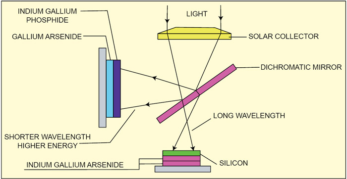
The sunlight can be split into different wavelengths by using a prism. These wavelengths can be used separately for different electricity-producing solar cells. This was done in 1970 and the rainbow cell so created had a very low efficiency as a lot of sunlight was lost. However, recent advances in optics have made it possible to manufacture dichromatic mirrors.
Mirrors made with dichromatic material can process and split the light with a 93 per cent efficiency. Fig. 3 shows the schematic diagram of such a device. White incident sunlight is split with the help of dichromatic mirror into two components—shorter wavelength with higher energy, and longer wavelength with lower energy. While the shorter-wavelength light is utilised in indium-/gallium-based solar cells, the longer-wavelength light is used in silicon-based cells. Under laboratory condition, the efficiency has been reported to reach 40 per cent. The goal of the manufacturing cost has been set to about Rs 140 per watt of energy (without government subsidy).
Solar cells that work at night
A new breed of solar cells that harvest energy at night could double the output of conventional panels. It sounds like an oxymoron, but a new breed of nanoscale light-sensitive antennae could soon make this possible, heralding a novel form of renewable energy.
Under ideal conditions, solar arrays of billions of tiny antennae can collect 84 per cent of incoming photons. A complete system of this new breed of electronic solar cells would have an overall efficiency of 46 per cent considering all losses, whereas the overall efficiency of the most modern silicon solar cells is stalled at 25 per cent. What is more, if the orientation of the panel with respect to the sun is wrong, light reflects off the silicon solar cell instead of being absorbed to generate power. The key to these new devices is their ability to harvest radiation (infrared).
Beyond the red end of the visible range, but at frequencies higher than of radar waves and microwaves, is the infrared region of the electromagnetic spectrum between 1012 and 5×10¹⁴Hz frequencies (or wavelengths from 0.1 to 7.5×10⁻⁵ centimetre). Nearly 50 per cent of the sun’s radiant energy is emitted in the infrared region, with the rest is primarily in the visible region.
Infrared is remitted by the earth’s surface after the sun goes down, meaning that these new-generation solar cell antennae can capture some energy even during the night. Unlike PV cells, which use photons to liberate electrons, the antennae resonate when hit by light waves, generating an alternating current that can be harnessed.
To build an array that could capture both visible and infrared radiations, multiple layers of antennae—with each layer tuned to a different optical frequency—are to be assembled. Further, two technological parameters are to be fulfilled. First, the antennae must be close to the size of the wavelength being captured, which in the case of the solar spectrum can be very small—from millimetres down to a few hundred nanometres. Second, the currents produced will be alternating at frequencies too high to be of use unless first converted into a steady current. The problem here is that silicon diodes, which are crucial to the conversion, typically don’t operate at the high frequencies required.
Both of these barriers are now broken. A technique for creating arrays of billions of antennae that are small enough to work with mid, near infrared and far ends of the infrared spectrum is developed. Current-conversion problem is tackled by creating novel diodes capable of handling high optical frequencies.
Semiconductor diodes act like valves, converting alternating current (AC) into direct current. To work with the new-generation antennae, these have to operate at the AC frequencies being received and match the conductive properties of the antenna. Semiconductors are ill-suited for this, as these tend to become less conductive when shrunk to the size of the antennae.
It is found that physical geometry of the device influences current flow. By creating asymmetry in the geometry of the diodes, it funnels electrons to flow only in one way. Nanoantennae are optical collection devices designed to absorb specific wavelengths that are proportional to the size and shape of the nanoantenna. Just like their bigger radio frequency counterparts, these have the advantage of limiting the incoming radiation to one mode with one polarisation.
Several different types of nanoantennae—such as dipole, bow-tie, spiral and log-periodic or microstrip antennae—are used to generate power from optical radiation to suit the specific wavelength. These can be used in the visible and invisible ranges. A nanoantenna is fabricated using electron-beam lithography and lift-off technique.
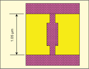
Typically, a dipole antenna element is made of 100nm-thick evaporated gold. A bolometer made of nickel is patterned at the feed end of the nanoantenna to serve as the detection mechanism. A pair of 200µm bond pads is patterned on both ends of the dipole antenna in order to provide biasing and obtain electricity. The device is fabricated on a silicon wafer with 200nm thermally grown silicon dioxide. An electron micrograph of the device is shown in Fig. 4.
Diamond power
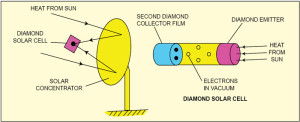
Diamond no bigger than a speck of dust might not interest a bank robber, but is turning out to be a physicist’s best friend. Diamond’s hardness and lustre have been prized for centuries, but when it is reduced to nanoscale size, other valuable properties of electronics emerge. Diamond films can make a new kind of solar cell that generates electricity by absorbing heat rather than visible light wavelength. The property is known as thermionic emission—the property of some materials to spit out electrons when heated. It turns out that ultra-thin diamond is better at this than most other materials.
The device is made of two thin films of diamond a few micrometres thick, which are separated by a vacuum a few hundred micrometres thick. A reflective dish is used to focus sunlight onto the device. As sunlight heats the outer diamond film (the emitter), the hottest most energetic electrons fly off. These travel across vacuum to a second diamond film (known as collector) that generates current.
A bank of such diamond-based solar concentrators can be made to exploit the sun’s energy to electric power. To make the diamond films work effectively, lithium atoms must be implanted into them. These atoms form positive charges near the film surface, which helps hot electrons leave.
Unfortunately, the very arrangement of carbon atoms that gives diamond its hardness makes it difficult to insert alien atoms. Lithium atoms seep extremely slowly in the hot diamond film. Hence lithium ions are used, which diffuse more easily throughout the structure.
The arrangement of a solar diamond thermoelectric generator device is shown in Fig. 5. A number of such devices arranged in arrays can be utilised to harvest the sun’s thermal energy in the form of electrical energy. The efficiency of this system is much more than the conventional solar thermal power generator.
The author has retired as deputy general manager, I/C, from MECON Limited


