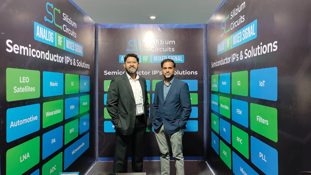
Discover the secrets behind successful IP development as we delve into innovative design strategies. Learn how to navigate the intricate balance between power efficiency and high performance. Sharad Bhowmick and Nidhi Agarwal from Electronics For You spoke to Dr Arun Ashok and Rijin John, Co-founders, Silizium Circuits and got some very interesting details…
Q. How does Silizium Circuits contribute to IP development?
A. Yes, we create something called ‘hard IPs.’ These are like small, important parts inside electronic devices, kind of like tiny chips within a bigger chip. Imagine opening up your electronic device and seeing many tiny chips working together to make it function. Companies like Intel, Renesas, or Infineon want to make their own chips, but stringent time to market necessitates more cooperation and collaboration. So, they seek partners like us who can provide these important parts, or IPs, to help them build their chips faster and better. This saves them time and money.

We are an Indian company, producing IPs that other companies can use in their products. We give them a graphic data system (GDS) file with all the necessary design details. It is a confidential file exclusively for their use, safeguarding our IPs. There are two types of IPs: one resembling the tiny electronic parts mentioned earlier, and the other is a special code called RTL logic. We offer both to assist companies in expediting their product development more efficiently.
Q. What tools and methods do you use to create hard IPs?
A. In our chip and IP design company, the technologies we use are connected to the foundry nodes that we collaborate with. Foundry nodes determine the smallest dimensions of structures within a chip. Our primary focus lies in analogue and RF technologies, ranging from 65 nanometres and upwards. We can work with nodes like 65nm, 130nm, and 180nm. We have agreements with various foundries enabling us to produce items using these nodes. However, when creating IP for clients, it must align with the technology they use. While we engage with nodes from 65nm and above for our in-house projects, we can also develop IP for clients using smaller nodes like 22nm or 28nm, based on their requirements.
Q. How do you ensure that the IP you design for different clients is compatible with their existing systems?
A. When commencing the design process, it all begins with a set of specifications or rules. These rules serve as standards that everyone adheres to. For example, when creating a product for navigation, there are rules both in India and internationally. Similarly, for GNSS (like GPS), there are diverse rules like NavIC, GPS, Galileo, and so on. These rules are mostly similar but may have small differences. So, when we create a product for a client, we make sure we follow the rules and requirements they give us.
Our design process proceeds from the top to the bottom. Initially, our system team dissects the specifications into smaller segments. Subsequently, our designers work on these segments individually, ensuring compliance with the specifications. We use special tools to simulate and test these segments for rule adherence. Once each segment is designed and tested, we integrate them to form the whole system. Subsequently, we conduct comprehensive testing to ensure optimal performance. Before commencing the design, we must understand how the product will be used, its power requirements, and other details. Multiple tests are conducted to valdate that everything aligns with our expectations from simulations. However, if our initial assumptions are wrong, real test results may significantly vary from our expectations.
Q. How do you address potential issues?
A. We address issues at the outset of the design process, not later. We cannot afford to spend three or four months designing something and then realise we overlooked factors like interference, noise, and other issues. For instance, if there’s a shared or noisy power supply, we must consider that from the project’s inception. Our approach involves not only designing the system but also creating test setups for various scenarios. We account for all these factors before finalising the design and progressing to subsequent stages.
Q. What is the smallest size that you have achieved?
A. Our silicon is like a tiny coil, about 2 millimetres in size. When producing prototypes, we use a chip with 32 pins because we need extra ports for testing and other purposes. However, for mass production, we aim to use a smaller version with perhaps 16 pins or even 4 pins, to enhance efficiency.


