

As a result, for the same energy quantum, time required for transfer continuously reduces as the voltage builds up across the capacitor from zero to the final value due to diminishing voltage quantum. Therefore it is not advisable to use a fixed frequency or fixed off-time switching supply. The drive waveform needs to be a variable frequency one with the off-time periods governed by the charge status of the energy-storage capacitor.
It can be mathematically proved that the size of voltage packet varies from V when the capacitor is fully discharged to [√N–√(N–1)]×V, where N is the number of packets required to charge the capacitor to the final value. If the off-time of the drive waveform could be varied or decreased to be more precise in accordance with the voltage build up across the capacitor, the power supply would operate at the highest possible conversion efficiency.
Fig. 2 shows the preferred block schematic arrangement of a capacitor-charging power supply configured around an externally-driven flyback converter.

The circuit is divided into two major parts, namely, the drive circuit and the feedback circuit. The drive circuit comprises a cascaded arrangement of a voltage-controlled oscillator (VCO), a monoshot circuit and a drive circuit. Output of VCO feeds the trigger input of the monoshot. The pulse width of the monoshot is chosen to be equal to the desired on-time of the switching device. The frequency of monoshot output and hence the off-time of the waveform is governed by the frequency of the VCO output, which in turn depends upon the voltage applied to its control input.
The drive circuit provides the required drive current and/or voltage depending upon the type of switching device used. The feedback circuit VCO output frequency is configured around a comparator and a subtractor. The comparator circuit is used to reset the monoshot circuit and therefore withdraw drive current from switching device as and when the output voltage reaches the desired output voltage.
The subtractor output controls the frequency of the VCO and therefore the off-time of the drive waveform to the switching device. The subtractor output in turn depends upon the voltage across the energy storage capacitor decreasing with increase in voltage.
Decrease in control voltage to VCO increases the output frequency, thereby reducing the off-time at the output of monoshot. What is important here is that the pattern of reduction of off-time is linearly related to the reduction of control voltage, which in turn is linearly related to increase in voltage across the capacitor. Thus off-time reduces in accordance with increase in the capacitor voltage. This design yields the most optimum results.
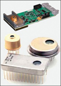
Compact capacitor-charging power supplies covering a range of input-output voltage and power output specifications are available from different manufacturers of laser electronics. One such unit intended for OEM applications is shown in Fig. 3.
Simmer power supply
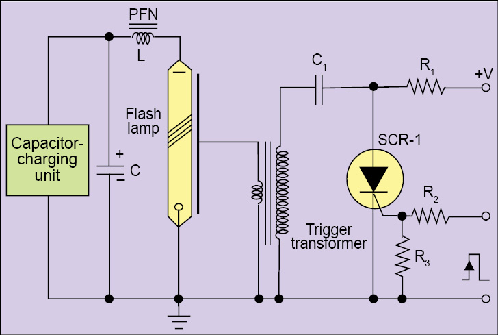
The simmer power supply maintains a steady-state partial ionisation of the flash lamp during the time the lamp is not flashing by maintaining a low keep-alive current though it. Simmer power supply must be designed with due consideration to I-V characteristics of the flash lamp. The simmer power supply is a high-voltage DC power supply producing an output voltage in the range of 800V to 1500V depending upon the characteristics of the flash lamp and the required magnitude of simmer current. A high-voltage trigger pulse, typically 10kV to 15kV, creates pre-ionisation before the simmer power supply can take over and deliver the keep-alive current through the flash lamp.
The output of the simmer power supply is applied to the flash lamp through a series resistor called ballast resistor. The magnitude of the simmer current therefore depends upon the difference between the simmer supply output voltage and voltage across the flash lamp in the simmer mode, and the value of the ballast resistance. The value of the ballast resistance should be slightly higher than the negative impedance offered by the flash lamp in the simmer regime.
Simmer power supply is generally designed around an externally-driven flyback converter topology with output power delivery capability equal to product of required open circuit output voltage and magnitude desired simmer current. Open circuit voltage is further equal to sum of voltage across the lamp in simmering condition and voltage drop across the ballast resistor. Fig. 4 shows simmer power supply interface with the flash lamp.
