In order to program a cell into ‘set’ (binary ‘1’) state, assuming it was previously in ‘reset’ (binary ‘0’) state, a low current is passed for a few tens of nanoseconds through the cell. The TiN heater heats up the phase-change material to a temperature above its crystallisation temperature (around 200ºC) but well below the melting temperature (around 600ºC). This causes the atoms of the glassy material to move and fall into energetically more favourable periodic positions. The material thus transforms to its crystalline phase that represents binary ‘1.’ This process transforms only a part of the entire material volume but the change is reflected in the increased amount of crystalline material after the annealing process, as seen in Fig. 2.
In order to go from the ‘set’ state to the ‘reset’ state, on the other hand, a short-duration large current pulse is passed through the cell, which heats above the melting point of the phase-change material and then cools down very quickly. The rapid cooling does not allow the atoms of the phase-change material to fall into an ordered arrangement, resulting in an amorphous glassy state that represents binary ‘0.’ This is how the cell is written to. The writing current waveforms are shown in Fig. 3.
In order to read the state of a memory cell, a small constant current is passed through the cell and the resulting voltage across it is measured. This reveals the resistance of the cell with a low resistance standing for binary ‘1’ and a high resistance indicating binary ‘0.’ The read current is too low to disturb the material state of the cell. The several hundreds of microamps required to change the state of a memory cell is a continuing concern and a lot of current development effort is being directed to reduce the power consumption of the PCM modules.

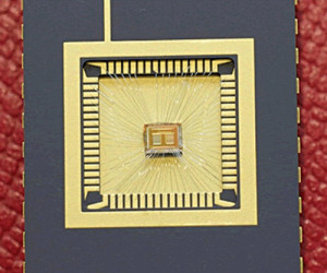
Once a cell has been programmed into its reset state by transforming the phase-change material to its amorphous state, the value of its resistance can steadily increase over time. This resistance drift was a big problem in the early days of PCM devices. Researchers at IBM research labs solved this problem by coming up with algorithms that measure the resistance drift of a block of contiguous cells and extract correct bit information by statistical sampling. Fig. 4 shows an experimental PCM device from IBM research.
More bang for the buck
In recent years, two principal strategies have been explored to increase the memory capacity of the PCM chips. One is to simply stack two or more layers of phase-change cell arrays to build a multilayer memory chip. Memory cells are arranged in two-dimensional arrays with cell selectors connected to word and bit lines in a cross-point switch arrangement. Although a feasible concept, this architecture has not been implemented as a working device yet.
The other, more viable route is to make use of the large resistance interval between amorphous and crystalline forms of phase-change materials by defining intermediate resistance levels as representing various bit combinations. Thus, in a four-level system, four resistance intervals can be used to represent 00, 01, 10 and 11. A byte, such as 10011010, can then be stored in four cells instead of eight, effectively doubling the memory capacity. More fine-grained resistance levels can be established by injecting carefully-controlled current pulses to heat and program the phase-change material in such a manner that a selected fraction of it changes its phase.
Researchers have shown that it is possible to make a 32-level phase-change memory system where each memory cell can store five bits. This is not a new concept as the present-day Flash memories rely on an eight-charge level scheme to store three bits per memory cell.
In the real world
Micron Technology offers a number of PCM devices with both serial and parallel data interfaces. The P5Q serial interface devices use serial peripheral interface (SPI) for reading and writing the binary data. These are available in 32Mb, 64Mb and 128Mb versions in 16-pin surface-mount packages with operating speeds as high as 66 MHz. Although there are 16 pins in these packages, only eight pins are electrically active. The logical organisation of these memories is such that they can be used as slow but non-volatile DRAM memories or as Flash memories.
Replacing Flash memories with PCM will improve memory access times due to reduced latencies and increased bandwidths. System reliability will also increase because Flash and other non-volatile memories usually require high programming voltages that can cause undesired electromagnetic interference effects.
It is very easy to use any of these devices in an embedded digital application as the standard SPI protocol, supported by most of the microprocessors and microcontrollers, is used for data storage and retrieval.
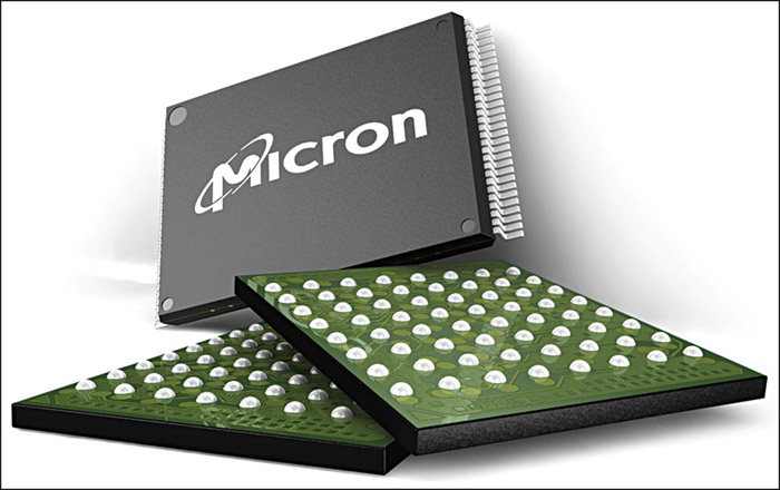
For more demanding, higher-speed applications, P8P parallel interface devices offer much higher-performance input/output (I/O) through parallel data transfer. These come in ball-grid array packages and are especially suitable for use in video card and server applications. Fig. 5 shows phase-change memory chips from Micron in both flat-pin and ball-grid array packages.
Thermal programming of PCM chips means that these devices cannot be pre-programmed before installing them on printed circuit boards as reflow soldering process will raise the chip temperature above crystallisation temperature of the phase-change material. Thus, after reflow soldering, all memory cells will be found in the set state, holding binary ‘1.’ This is even more certain with the new lead-free soldering process that operates at a higher temperature than the earlier one. This essentially means that PCMs have to be loaded with their content after board assembly, through an appropriate in-system programming interface.
Phase-change materials are widely used for re-writable non-volatile digital storage in optical disks. Re-writable CDs, DVDs and Blu-ray disks utilise a coating of phase-change material in which 0’s and 1’s are written thermally by a focused laser beam. The two states have different reflectivity and thus can be read by bouncing a laser beam off the recorded spots.
The electronic phase-change memories that take advantage of the difference in resistivity rather than reflectivity of the two phases of materials like GST are, however, only now beginning to appear, with Micron being the first company to offer parts that are in full production. As higher-capacity devices make their appearance, this memory technology is certain to replace NOR and NAND Flash memory in applications such as mobile phones, MP3 players, tablets and even computer servers. Technology analysts are forecasting that in the next two to four years, PCM chips and modules will drastically change the memory landscape, enabling lower-cost but higher-performance digital products of the future.
The author is working as a technology officer with Electrospell Ltd, UK