Electronic devices manufactured today are far more complex than were five years ago in terms of processing power, power consumption, memory, area and performance. To keep up with the market demand for higher bandwidth, more memory and lower power consumption in electronic products, electronics design automation (EDA) companies are rolling out valuable features in their range of software tools for designing electronic chips and systems in a faster, better and cost-effective manner.
EDA tools are also moving to a secure cloud environment, which could lower capital and operation expenditure. More on that and other interesting developments in EDA tools in the following sections.
Tools for system-level design
With the proliferation of the Internet of Things (IoT), an open, connected and scalable software tool can be used by developers to accelerate system-level design and verification. Many EDA companies provide comprehensive tools that provide high throughput and quick debugging and compilation. They are also adding new features to boost ease of use and adaptability of the software.

New features in some of the tools for system-level design and verification have been highlighted below. These allow engineers to execute design optimisations swiftly and effectively.
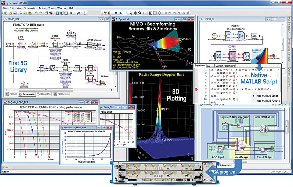
SystemVue. System architects, designers and verifiers mostly use electronic system-level design (ESL) tools to innovate the physical layer (PHY) of next-generation communication systems. It is important to have the right tool to design and validate the PHY layer of communication systems that simplifies this challenging task.
Usually ESL tools iterate the baseband and radio frequency (RF) designs separately in a system. Keysight’s SystemVue validates the entire system at an early stage and then co-verifies it at each step in the process. Common test benches are reused throughout the model based design flow, which reduces design time and verification effort.
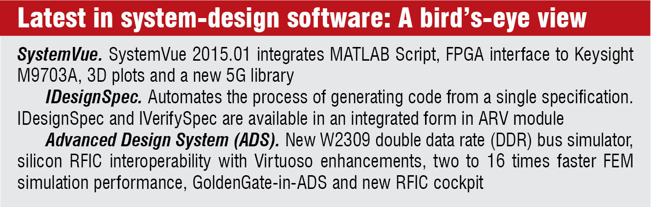
The latest release, SystemVue 2015.01, includes a module from MathWorks, MATLAB Script, which replaces mathlang equation parser in earlier versions. Equipped with locally-licensed copies of MATLAB, this module executes MATLAB models from within SystemVue. With updates to almost all libraries and add-ons, a new 5G library has also been incorporated. Instrument support and simulation have been expanded for wide bandwidth systems, especially for radar, 5G and satellite.
Another key feature included is a field programmable gate array (FPGA) programming interface for the M9703A real-time digitiser.
IDesignSpec. Modern systems on chips (SoCs) are quite complex and include a lot of functionality. Specifically speaking, Rinku Singh, design engineer, Agnisys says, “Register and memory-map definitions are becoming tedious, consuming significant implementation and verification time.” Agnisys’ IDesignSpec helps designers to capture register specification and generate the desired code.
Engineers manually read the specification and code RTL or C header files, which is highly undesirable as it is tedious, mundane and costly in terms of both time and resources. In the latest version, IDesignSpec automates this process of generating code from a single specification. The specification itself may be split over a number of individual documents or files.

“Agnisys recently launched Automatic Register Verification (ARV) module, where two separate tools (IDesignSpec and IVerifySpec) are available in an integrated form,” notes Singh. He adds, “IDesignSpec generates Universal Verification Methodology (UVM) environment and custom sequences, whereas IVerifySpec generates the verification plan, imports the existing plan, simulation vendor specific plans and annotated simulation results on to the plan.”
There are some features that were earlier optional for users to use, but in the latest version these work as default. Singh informs, “Tool Command Language Application Programmer’s Interface (TCL API) was optional in an earlier version, but it is now included by default. It helps users create their own outputs from the specification.” He adds, “The latest version completely supports several industry-standard buses like Advanced eXtensible Interface (AXI), Advanced High-performance Bus (AHB), AHB3Lite, Open Core Protocol (OCP), Avalon and Wishbone. This ensures that users can create SoCs with ease.”
ADS. The newest release of Advanced Design System (ADS) 2015.01 includes various improvements over the earlier version. This tool from Keysight Technologies typically covers the complete design flow of a product to manufacturing and is suitable for board, module and system designers.
Silicon radio frequency integrated circuit (RFIC) interoperability with Virtuoso enhancements provides designers with a schematic interoperable process design kit (PDK) as well as pcell support.
Improvements in finite element (FEM) simulation enable up to 16 times faster performance. There are also several layouts and layout verification improvements implemented in this version such as polymorphic interconnect modelling, layout interconnect design and faster layout viewing, to name a few.
Tools for system-level verification
Developers and integrators require verification tools to ensure that product specifications have been accurately tested and implemented. Using the latest in methodologies, new developments in verification tools look to increase the overall quality of the final product.
MATLAB and Simulink. Engineers today are using FPGAs for prototyping and algorithm acceleration. These can be realised with the help of system-level design and verification tools like MATLAB and Simulink, by quickly prototyping their algorithms on FPGAs.
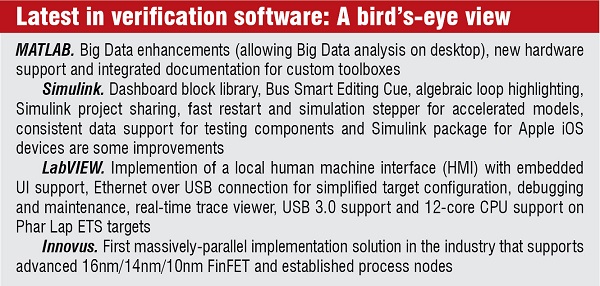
In the latest release of MATLAB, many new features have been included. It comprises a new graphics system and capability to analyse Big Data on a personal computer, after which it can be scaled to Hadoop.
Engineers can also pack custom MATLAB toolboxes into a single, installable file, and manage and control code within the MATLAB desktop.
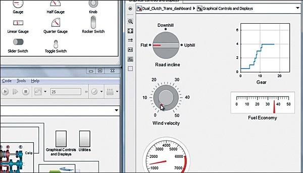
Simulink’s recent update enables engineers to test simulations with intuitive graphical displays and controls. With Bus Smart Editing Cue, it is now possible to combine signals into a bus signal and select specific signals or the entire bus can be accessed.
Project sharing and collaboration has been made easier with a share option. Users can share projects via GitHub, MATLAB toolbox and email, which is currently limited to Windows operating system (OS) only. Simulink also extends support to Apple iOS devices. This allows developers to create an app, which runs Simulink algorithms and models on iOS platforms.
LabVIEW. Engineers use system design tools to simplify complexity and for efficient hardware integration. Selecting the right design tool is the key to reduce development complexity and costs. Another popular tool, LabVIEW, recently got an upgrade that enables engineers to build better embedded monitoring and control systems, and make insightful data-driven decisions.
LabVIEW 2014 has a variety of enhancements made. For instance, in block diagrams, it automatically creates a shift register when a user places For loop or While loop around the existing code.
For a particular case structure, it is now possible to replace an input tunnel with the case selector. Earlier, DataPlugins were to be downloaded manually and installed, whereas in the latest version, one can directly search, install and update DataPlugins.
There have been other enhancements to LabVIEW environment, application builder, Web services and front panel as well.
Innovus. Increasingly, developers are turning to hardware/software co-design and co-verification, concurrently designing and verifying hardware and software components of the system design, to deliver on more demanding time-to-market requirements, observes Vishal Abrol, senior group director, Field Engineering, Cadence Design Systems (India) Pvt Ltd. He says, “Concurrent design and verification allows for software development to begin before silicon is available, often before it is frozen, which can shave months off the software development schedule.”
Launched in March 2015, Innovus Implementation System is for system companies that are working on complex, advanced node designs and face conflicting challenges around meeting requirements for power, performance and area (PPA) as well as turn-around time (TAT).
Abrol says, “It becomes very difficult to achieve the best power performance with maximum productivity without compromising the outcome of either of these requirements. Innovus Implementation System provides a typical 10 to 20 per cent production-proven advantage in the PPA of the design, along with an up to 10 times TAT and capacity gain.”
He adds, “The platform is the industry’s first massively-parallel implementation solution. It is built on a next-generation platform with several integrations that result in an easy-to-use core implementation and sign-off flow that facilitates better engineering productivity.”
Tools for board-level design
For every electronic product, a printed circuit board (PCB) is like its central nervous system, mechanically supporting it and electrically connecting electronic components mounted on the board. And, designers look to create a PCB that is competent in the first run. Therefore it is of paramount importance to design quality PCBs with the help of standard design tools in an efficient and cost-effective manner.
Tools in the market that look to tackle most of the complex design challenges and latest developments in some of these tools for board-level designing are featured below:
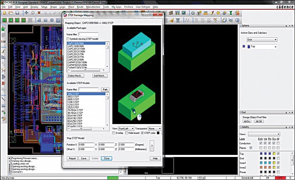
OrCAD. In July 2014, Cadence introduced three new additions to its OrCAD product line to accelerate the mainstream PCB design process and provide a significant boost to productivity and efficiency.
Abrol says, “The new OrCAD products include OrCAD Engineering Data Management (EDM), a comprehensive collaboration and management environment for OrCAD Capture; OrCAD Library Builder, a rapid automated part builder; and OrCAD Documentation Editor, an intelligent, automated PCB documentation environment.”
PADS. Acquisition of PADS has strengthened Mentor Graphics’ tools for board-level design. Recently in April, Mentor Graphics released three new tiers of the PADS offerings—PADS Standard, PADS Standard Plus and PADS Professional.
Standard and Standard Plus versions have the same graphical user interface (GUI) as the earlier versions to make it easier for the user to switch and adapt. These suites have been enhanced with additional capabilities to incorporate design archiving, common constraint management, integrated design and additional analysis capabilities.
But PADS Professional version has a completely different GUI as it is built on Xpedition design technology from Mentor Graphics. It is targeted at professionals who require more power and capabilities for highly-complex designs.
Later in the year, a 2D/3D co-design solution will be introduced along with other new features.
CADSTAR. The latest version of this single-board design tool from Zuken enhances design efficiency to meet the requirements of today’s high-speed designs, as well as routing functionality and group handling with its new features. Items contained within a group can be selected and modified without first ungrouping these, which was not possible earlier. This simple improvement will provide users with more time to focus on their designs and improve design quality as ungrouping items poses a risk of regrouping these into a different configuration, informed Jeroen Leinders, CADSTAR worldwide sales manager, in a release.
Now, it is also possible to enter exact length and coordinate values while creating shapes in CADSTAR design editor, resulting in time saving and ease of use.
Place and Route (PR) editor supports impedance balanced routing, which accelerates implementation of high-speed interfaces.
CR-8000. CR-8000 2015 aims at empowering team collaboration for single-board and multi-board designs. In this version, combination of IC packaging and 3D multi-board design enables design teams to make products faster with a lower occurrence of design errors.
CR-8000 System Planner has enhanced module based and hierarchical system design capabilities, making it straightforward for engineers from all over the world to contribute to system design.
Today, reuse is an important part of the design process. Design Gateway allows constraints design and reuse by multiple team members. To support global standards, this software tool now creates output to IPC-2581B standard.
Tools for chip design
ANSYS RedHawk. ANSYS RedHawk now supports Distributed Machine Processing (DMP). DMP technology enables designers to run on-chip power integrity simulations for large SoCs with fast turn-around time. Vinayakam Subramanian, area technical manager, ANSYS says, “With designs moving to advanced technology nodes and increasing addition of functions to ICs, the complexity of the chip Power Delivery Network (PDN) increases significantly.” However, he adds, “Design cycles get shorter due to faster time-to-market constraints. RedHawk’s DMP capability enables users to simulate and sign-off complex SoC on advanced technology nodes with fast turn-around times.” DMP leverages SSH and LSF infrastructure on Unix networks to distribute the simulation over a span of machines on the network – once the distributed simulation is complete, results are collected from all the machines and displayed on a single RedHawk GUI for ease of use.
ANSYS RedHawk also supports chip package co-analysis in the same environment. Subramanian says, “User can import both chip and package layouts into RedHawk GUI and is able to co-visualize both layouts side-by-side in the same environment. Package-aware on-chip power integrity simulations can be done in the same RedHawk session, without the need to resort to another tool just for package modeling.” He adds, “Once package-aware chip analysis is done, the bump current data can be used to drive package co-simulation as well in the same GUI.”
Apart from updates to existing tools, there are some new software on the block, too.
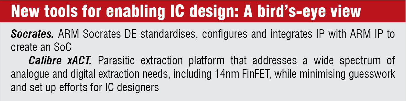
Socrates. ARM recently launched a software suite that aims to reduce the SoC integration time from months to days, thereby simplifying and accelerating system integration. Socrates design environment (DE), one of the tools in the package, can be used by designers to standardise any semiconductor intellectual property (IP) into IEEE1685-2009 standard, making it integration-ready.
Apart from enabling IP standardisation, Socrates also allows automated, intelligent and fast IP integration. To ensure that the system is feasible, this tools runs design rule checks, also enabling designers to visualise each stage of the design.
CoreSight Creator, CoreLink Creator and AMBA Designer are the other tools that are part of this software suite.
Calibre xACT. With the aim to reduce set up efforts and trial and error methods for IC designers, this new addition to Mentor Graphics’ Calibre software suite takes care of a wide range of analogue and digital extraction requirements, including 14nm fin-shaped field effect transistor (FinFET).
IC designers working at advanced nodes face quite a lot of challenges with these smaller nodes like extracting inductive, capacitive and resistive values of a design. This new parasitic extraction platform also works with Synopsys’ and Cadence’s verification and physical design software. The newest IC processes can achieve better accuracy with Caliber xACT’s ability to use a single-rule deck for a variety of extraction applications, and faster performance and TAT without having to manually alter their tool’s configuration.
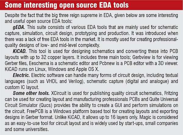
With growing demand, open source could dominate EDA, too
Open source is everywhere—in majority of programming languages, integrated development environment (IDE), OSes and everyday tools. But open source tools have not yet penetrated the EDA domain (especially for synthesis and simulation) in the same manner as these have in other arenas. The reason could probably be the size of the EDA industry and users of EDA tools.
Another reason could be the lack of software developers designing EDA tools. Also, there are three major companies, Mentor Graphics, Synopsys and Cadence, which provide competitive software. If there exists a strong, growing need for open source EDA software by design engineers, then that demand should drive developers to improve the quality of these open source tools in the future.