
Due to the advancement of the semiconductor industry, the technology node keeps on decreasing. This leads to lesser core voltage and higher current requirement. Also, the voltage regulators need to have good transient performance due to fast load switching. It is very challenging for the power domain engineers to design such very low conversion ratio high current converters with desired transient response, efficiency and other performance indexes. On the other hand, when supplying power for different ICs on a board with different voltage and current requirement, some power delivery architecture needs to be followed. Special care is required for these high frequency components, as RF noise can screw up the whole power delivery system. Grounding is another part for power delivery system. Proper grounding system is necessary, otherwise the board may not work as intended. Special attention needs to be paid on layout design too, as it is going to decide the overall system performance. Let’s look at some power supply design tips starting with regulator design guidelines before going into power delivery architecture.
Power supply design: regulator guidelines
Linear voltage regulators can be used when it requires to stepping down the input voltage to a regulated output voltage. These are having very good transient performance (higher bandwidth) and very low ripple at the output voltage. It also generates very low EMI. So, linear regulators are good choice for supplying RF components. The only bad thing about linear regulator is its efficiency. Efficiency reduces drastically as the conversion ratio (output voltage/input voltage) decreases (i.e. for fixed 5V input efficiency reduces from 80% to 50% as the output voltage changes from 4V to 2.5V).
For higher conversion ratio, linear regulators are better choice than switching regulators. But as the conversion ration decreases, people tend to use switching regulators if the other above mentioned requirements are not so stringent. Low dropout regulator (LDO) is a special variant of linear regulator can be used when the conversion ratio is very high. It is also useful for declining input voltage (i.e. discharging battery).
Design guidelines for linear regulators
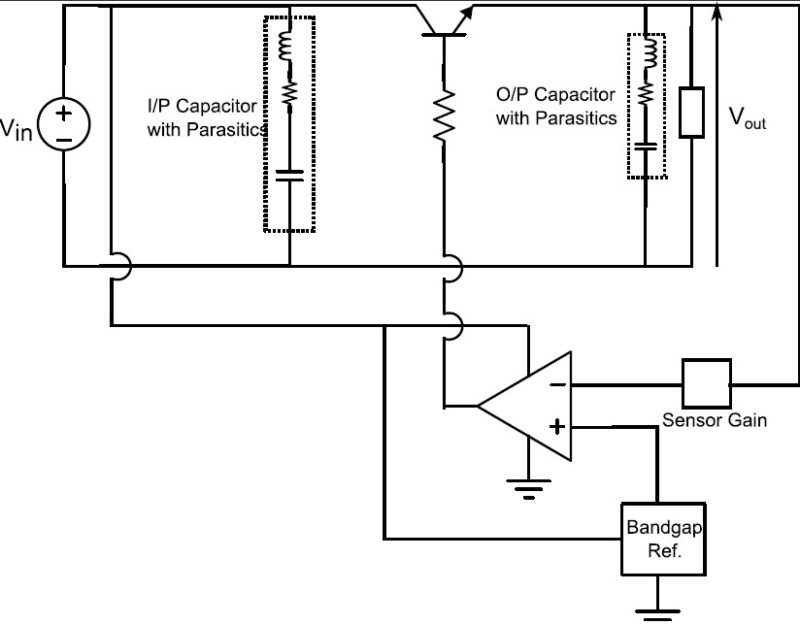
A linear regulator must be selected based on the load current, input and output voltage requirements. As the transistor is operated in linear region, there will be certain amount of power dissipation on the pass transistor. So, thermal design needs to be done so that the die temperature should not exceed 75 % of the maximum rated limit. The over current limit should be set such a way that linear regulator should not cross its safe operating area (SOA).
Other performance indices for linear regulators are stability and transient response, line regulation and load regulation, power supply rejection ratio (PSRR) and efficiency.

- Stability and transient response is decided by the open loop frequency response of the linear regulator. The load capacitance in conjunction with output load adds a pole and the ESR of the output capacitor in conjunction with output capacitance adds a zero to the open loop transfer function. Internal pass transistor and error amplifier can be modelled combined as a first order system. The open loop frequency response of the overall is largely depends upon the selection of output capacitor. Very low or high value of ESR makes the system unstable. So, firstly an optimum ESR value needs to be chosen for proper operation. Secondly instead of using simple resistive divider for voltage feedback, resistive capacitive divider network would be better choice and helps to tune the open loop frequency response to achieve stability and better transient performance for wide range of operating load.
- Line regulation signifies the change in output voltage due to input supply voltage variation. Similarly, load regulation signifies the change in output voltage due to load variation. These data are available on the datasheet and should be well under the system requirements.
- PSRR measures the AC coupling between the input supply voltage on output voltage. Low frequency input supply voltage ripple couples with bandgap reference generator and error amplifier. High frequency ripple finds path through capacitive coupling between drain and source (or collector and emitter) of the pass transistor. The bandwidth of the system limits the regulation at high frequencies too. Feedforward power supply noise rejection scheme can be adapted to make the system immune against power supply noise.
- The efficiency of the linear regulator depends upon the dropout voltage. It’s good to use it when the dropout voltage is less.
Regulations with switching regulator
These guidelines go well for linear regulators however the story is a bit different for switching regulators. Switching mode regulator, transistors are operated in switching mode instead of linear mode. This helps to achieve higher efficiency, lower power dissipation and higher power density (small size) than linear voltage regulators. But nothing comes for free. There is performance reduction in terms of transient response, output voltage ripple and EMI generation.
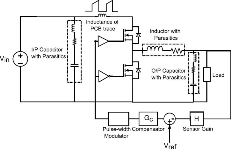
There are different topologies available for switching regulators. Most fundamentals are buck topology, boost topology and buck-boost topology. MOSFET is mostly used for lower voltage application. Synchronous switching is used mostly because of higher efficiency. Here a buck topology is considered. But all the things are still valid with different topologies also.
Design Guidelines for switching regulators
Efficiency is an important parameter to judge the system performance. Efficiency can be improved by reducing the losses. The main source of losses for switching regulators are conduction and switching loss in the upper MOSFET, conduction loss in the channel and body diode of bottom MOSFET, conduction and magnetic loss in the inductor, loss in the filter capacitors.

- Conduction loss in the MOSFET depends upon the on-state resistance (Ron) value and the current flowing through the device.

MOSFET static model (a) turn on, (b) turn off On state resistance is proportional to the blocking voltage of the MOSFET. The blocking voltage of the MOSFET is decided based on DC bus voltage. Designer always choose the device with blocking voltage rating higher than the DC bus voltage. This is because of two reasons mainly: there is an overvoltage across the switch during turn off and designer always deigns with some factor of safety. But there should not be a high percentage of factor of safety. It will increase the conduction loss.
- Switching loss in upper MOSFET happens during switching transitions (switching on and switching off transitions) as the MOSFET switching is not ideal.
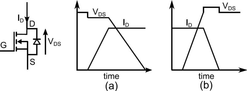 This loss is proportional to the switching frequency, instantaneous current trough the device and the voltage across the device during the off-state condition. The parasitic capacitance values change proportionally with the voltage and current rating of the device. So, the switching loss will increase. On state resistance drops when a high current MOSFET is selected. But it will increase the switching loss. So, there should be an optimum value which needs to be decided by the designer.
 - As soon as the upper MOSFET is turned off, inductor current starts to freewheel through the body diode of the bottom MOSFET. A dead-time is provided in between the switching of two MOSFETs to avoid cross conduction. During dead-time, inductor current fully flows through the body diode. As it is not optimized for conduction loss, a large amount of power loss occurs here. So, dead time value should not be too low such that cross conduction happens. From the other angle, it should not be too high, otherwise it ends up with bad system efficiency.
- After the dead-time, bottom MOSFET is gated, channel takes over most of the current flowing through the body diode and power loss reduces.
- Conduction loss happens in the induction mostly because of its DCR. Increasing the cross-sectional area of the conductor reduces the DCR value. But it will increase the size of the inductor. There is another component of loss in the inductor comes from magnetic loss when iron core inductors are used. Air core inductors are free from magnetic loss and used for switching regulators with higher switching frequency.
- The output capacitive filter is not ideal and it has some ESR. There will be small amount of power loss occurs there. Capacitor with very low ESR must be selected to get a good efficiency.
- The system efficiency for light load condition is very low when only pulse width modulation (PWM) is used. So, for light load condition regulator can be switched to pulse frequency modulation (PFM) for better efficiency.
- Switching frequency decides the filter size. Higher switching frequency reduces the filter size and simultaneously the losses in the filter. But it increases switching losses and requires larger board size or heat sink to dissipate the heat generated. It also reduces the system efficiency. So, the switching frequency selection is a tough job for the designer and needs to be selected judiciously to get the optimum performance out of the regulator. Generally, for point of load regulator typical switching frequency ranging from 100 kHz to 1 or 2 MHz.
- For a constant switching frequency, smaller inductance gives larger ripple and larger RMS current on the MOSFET. This increases the conduction loss in the upper MOSFET. On the other hand, high inductance gives larger inductor size and higher DCR value. Generally, 10-60% current ripple is permissible and selected depends upon the application.
- The inductor in any switching regulator topology acts as a constant current source. When the MOSFET switches, depending upon the topology, there will be pulsating switching current in the input or output or both. i.e. for buck topology there will be pulsating switching current flowing in the input. So, the input capacitor sees very high ripple current. So, capacitor with very low ESR must be selected as the RMS current is high. As the switching current is flowing through the input capacitor and the MOSFET for buck topology, input capacitor should have a very low ESL value and it should be placed very close to the power MOSFETs. The input capacitor should have some high frequency ceramic capacitors (most likely X5R or X7R) in parallel with bulk ceramic or electrolytic capacitors such that impedance over wide frequency range should be low.
For buck topology, the output current is continuous. But it is not constant current, there is ripple in it. AC part of this current is flowing through the output capacitor. So, to reduce the output ripple voltage, ESR and ESL of output capacitor needs to be low. So, output capacitor should also have some high frequency ceramic capacitors in parallel with bulk ceramic or electrolytic capacitors such that overall ESR and ESL value is low. For boost and buck-boost topologies, the output current is switching pulsating current. So, capacitor selection demands special attention.
- Good transient performance in supply system is always required for embedded applications. For faster response against load transient and input voltage disturbance, system bandwidth should be high. But system bandwidth is restricted by the switching frequency. Generally, system bandwidth should be at least one fifth times of switching frequency. Selection of higher switching frequency helps in faster transient response. Transfer function of buck topology is fairly simple. It has double pole at LC oscillation frequency and a zero added by output filter in conjunction with capacitor ESR. A compensator network needs to be designed properly to get proper gain and phase margins. A lower phase margin leads to oscillation whereas a high value of phase margin makes the system response slower. Phase margin needs to be something around 30-45 degree for proper operation. For boost and buck-boost topologies, there is a right-hand side zero in the transfer function which will give phase loss and may cause instability for light load conditions. Special attention needs to be paid during the design of compensators for such regulators.
- Switching transition may cause EMI problems if the transition time is too low. By increasing the value of gate resistance of the MOSFETs, transition times can be increased and ultimately it reduces EMI. Though the bad part is it increases switching loss.
Power Delivery Architecture
Different voltage is required for different components on a PCB. Different voltage rails are required to supply those components. So, proper power delivery architecture is required. Power delivery architecture can be adopted depending upon three different criteria: Efficiency, power density and cost. Different architectures have been discussed here.
- A typical power delivery architecture consists of a single front end regulator supplying all the different voltage rails (i.e. multichannel buck regulator).
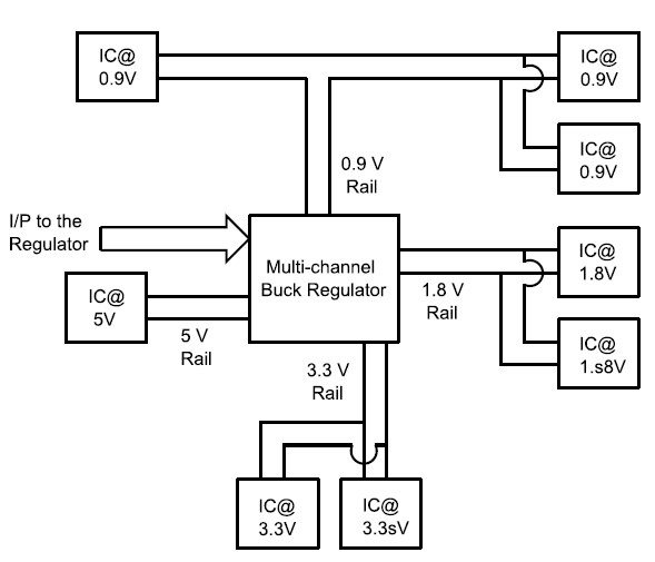
Typical Power Delivery Architecture Instead of using a single multichannel buck regulator, multiple ICs can also be used. But if too many voltage rails are required, using separate IC for each voltage rail increases the BOM cost and reduces power density. The main disadvantage with this architecture is that if the distance between the component supply node is far from the regulated voltage node, there will be IR drop when the component draws current. Now, i.e. if the component requires 0.9 V input and due to IR drop the voltage drop of 0.3 V happens, then the component might not be functional. Over which there is always chance of ground bounce and cross coupling.
- Nowadays people are using point of load distributed bus architecture.
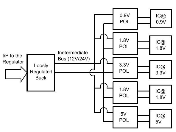
Point of Load Distributed Bus Architecture This architecture uses two step conversion process. First the input voltage is converted to a known loosely regulated voltage (i.e. 12 V for 24 V). This voltage reaches near to the components through distributed bus. There near the component, second step of conversion happens (i.e. 12 V to 3.3 V). The output voltage of the second stage is tightly regulated. This architecture will increase the BOM cost. This architecture suffers very less from ground bounce and cross coupling problems.
Grounding and Layout guidelines
PCB for embedded application contains analog, digital and RF components. So, grounding should be proper. Otherwise there can be interference between them which may leads to system response far from intended. Components need to be classified according to their functionality and same type of components should be connected to the same ground. Ferrite bead needs to be placed in between different grounds (i.e. analog and digital ground). Ferrite beads need to be designed such that it can provide very high attenuation for the interfering signals. So, the current will flow through the intended path. It reduces the loop area for go and return of any signal and simultaneously reduces the radiated EMI.
There are two different philosophies regarding signal grounding schemes
- Single point grounding and
- Multipoint grounding
- A single point ground system is one in which subsystem ground returns are tied to a single point within the subsystem.
Daisy Chain Grounding There are two possible way to do that. The first one is daisy chain approach. This technique has a problem of permitting common impedance coupling between two subsystems. The second approach is the star connection approach. But in this case also,
Star Grounding individual ground conductors will have some impedance depend on the length of the connections. In a distributed system, these connection wires may need to be long so that it can be connected to a single point. This increases the ground impedance as well as the loop area. So, it will produce coupling between subsystems.
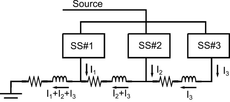
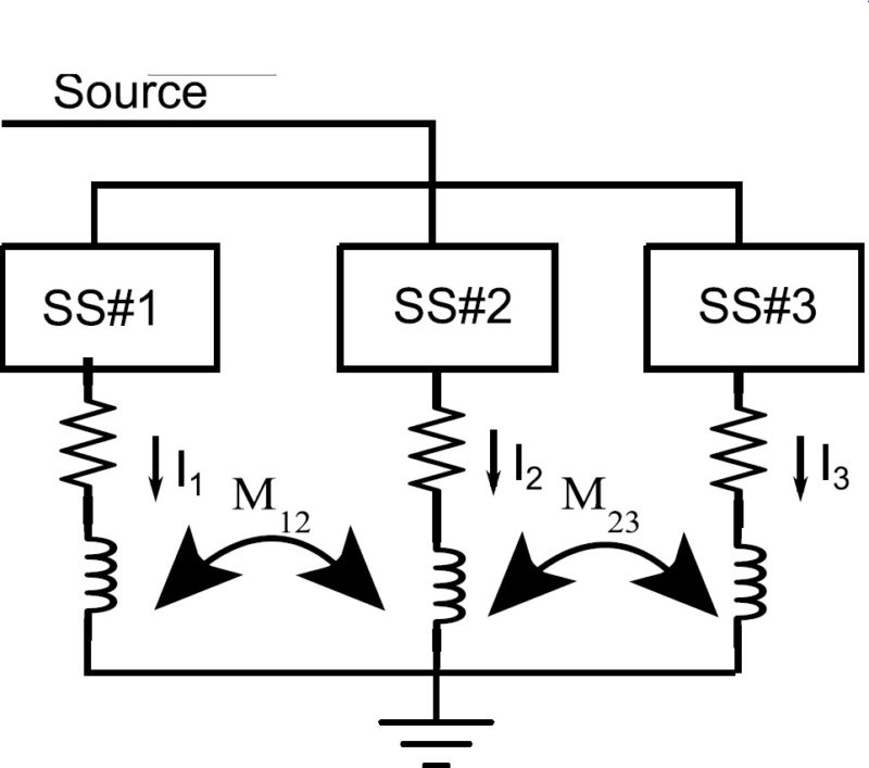
- In multipoint ground system, a large conducting plate serves as the return of ground current.
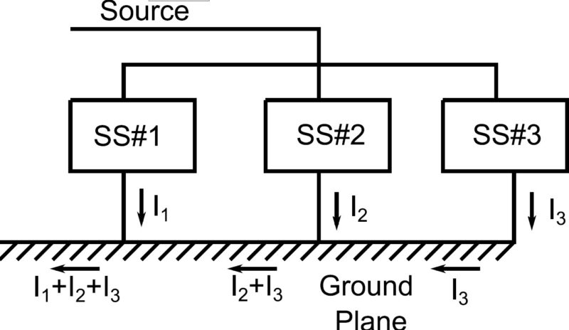
Multipoint Grounding Individual grounds of different subsystems are connected at different points to this plate. The main assumption for multipoint ground system is that impedance between points of ground return plate to which individual subsystem grounds are connected has very low impedance at the frequency of interest.
When two subsystems are connected at ground points which are far away, due to high frequency current flowing through the ground, there will be voltage drop across two grounds. So, it is required to put high frequency decoupling capacitor near to every subsystem such that high frequency is supplied by these decoupling capacitor locally.


Hlo
I actually need to design a power supply of 12v,53a.
Can you please help me.
muy bueno muchas gracias por compartir
Gracias por tus comentarios