


 Presented here is a simple circuit for switching your CCTV camera outputs sequentially.It switches four video and audio channels sequentially, one at a time.
Circuit and working
Fig. 1 shows the circuit diagram of the four-channel video and audio sequencer. It is built around NE555 timer (IC1), 4017B decade counter (IC2), four npn transistors BC547 (T1-T4), four DPDT relays (RL1-RL4) and a few other components.

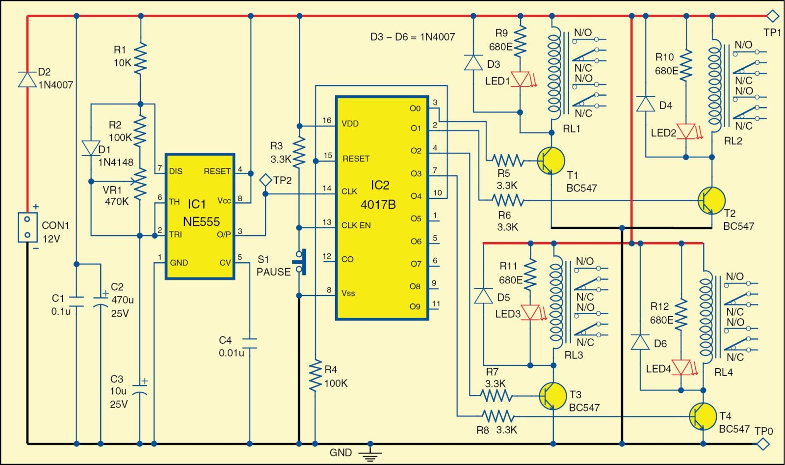
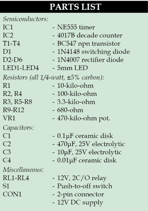 IC1 is configured as an astable multivibrator. The frequency of its pulse and on/off times are determined by resistors R1 and R2, potmeter VR1 and capacitor C3. Diode D1 makes R1 the only resistor controlling the charging of C3, while R2 and VR1 alone control its discharge through discharge pin 7. Output of IC1 from pin 3, which is a narrow, rectangular pulse train, is applied to pin 14 of IC2 (clock in), which starts counting. The second clock input (pin 13) of IC2 is grounded through switch S1. Outputs O0 through O3 of IC2 turn-on transistors T1 through T4 in a sequence, one at a time. Each transistor controls an associated relay. Each relay, in turn, switches on/off the video and audio lines coming from each camera.
The time period for switching between each camera is controlled by R1, R2, VR1 and C3. VR1 lets you adjust the time period over a range of one to five seconds per view. If you need a longer cameras-on time before changing the scene, change the value of VR1 to, say, 1M, or change C3 to 22µF.
IC2 is a decade counter, which means that first, output O0 goes high (after reset), followed by output O1 after the first clock pulse, then output O2 goes high after the second pulse, and so on, all the way up to O9.
After the tenth pulse, it starts again from O0 and the cycle repeats. However, in this circuit, use of reset function at pin 15 forces the chip to repeat the cycle after the fourth pulse, instead of the tenth pulse. This is done by connecting output O4 (pin 10) to reset pin.
Each output (O0 through O4) of IC2 goes high sequentially, and the cycle repeats. Around 12V is available across each output pin (O0 through O4), whenever it goes high. Output pulses turn-on transistors T1 through T4 sequentially, via base-current-limiting resistors R5 through R8.
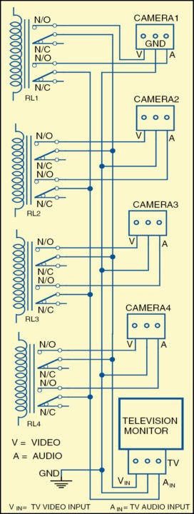
An LED with a current-limiting resistor is connected across each relay coil. This indicates the working of the circuit. A pair of each relay contact is used to switch the video signal, while the other pair is used to switch the audio signal coming from the camera.
Switch S1 is used as a pause function. The pause facility is provided to stop the counting in IC2, so that you can hold and view a particular channel. During the pause action, we simply break the circuit by disconnecting pin 13 from the ground and allow resistor R3 to pull it high. The pause continues as long as you keep the button pressed. As soon as you release the switch, pin 13 is connected to the ground again, which resumes the counting, and the video and audio sequencing continues.
Construction and testing
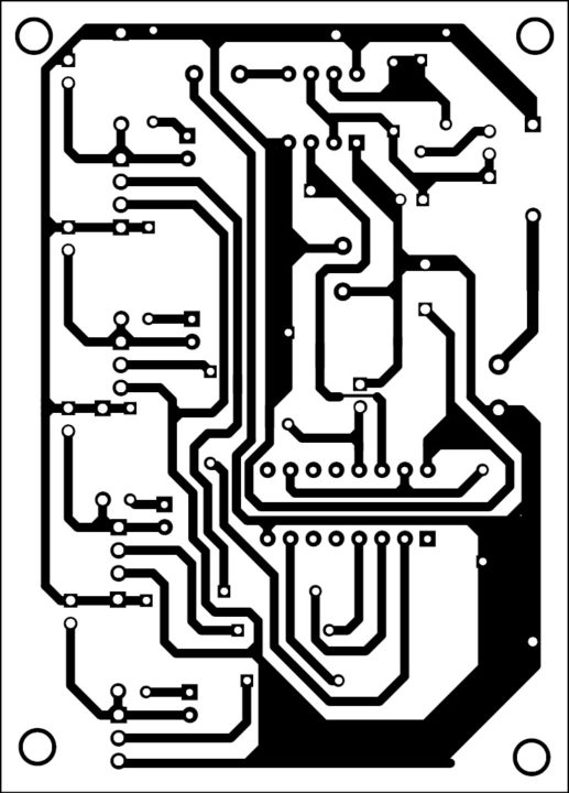
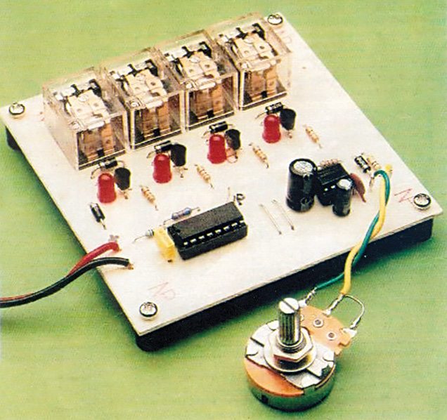
A single-side PCB of the four-channel video and audio sequencer is shown in Fig. 2 and its component layout in Fig. 3. After assembling the circuit on the PCB, enclose it in a suitable plastic box.
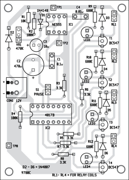
Switch S1, potentiometer VR1 and the relays should not be mounted on the PCB.
Connect the relays to respective connecting points (RL1 through RL4) provided in the PCB. The connection diagram for interfacing the cameras with relays and the TV monitor is shown in Fig. 4.
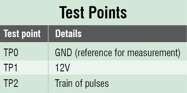
For troubleshooting, verify the parameters at various test points as shown in the table.
Download PCB and Component Layout PDFs: click here
The author is an electronics hobbyist.
This article was first published on 17 December 2015 and was updated on 2 April 2020.
I have learnt alot on this information i apprieate your efforts toward comming up with explanation on video sequencer for four channel. God bless you.
Thank you for your feedback.
What was the failure of the article of 17 December 2015
Hi Shabani, we have added some of the reference link articles within the project for a better understanding of the project.