In the first part of this article, we had described the main features of the AVR microcontroller and the hardware/software required for an AT-PROG programmer board interfaced to the printer port of a PC. Further, we explained the methods for message display on a liquid crystal display (LCD).
This part dwells on the architecture of ATmega8535 along with application programs exploiting its important features for embedded control.
Architecture of ATmega8535
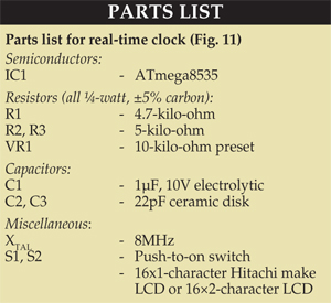
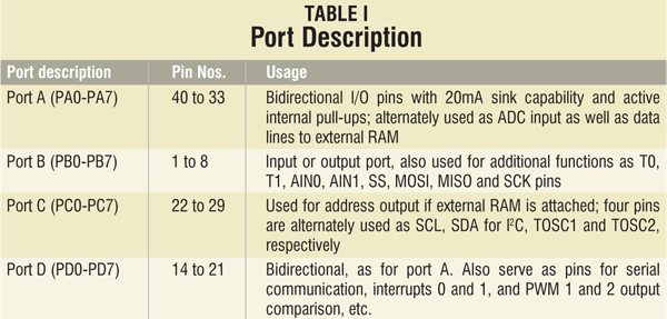
Pin configuration of ATmega8535 was shown in Fig. 1 of Part 1. The device has ports for input/output, interrupts, serial communication and various others functions. There are a total of 32 pins, which are arranged as ‘A,’ ‘B,’ ‘C’ and ‘D’ ports for various functions as shown in Table I.

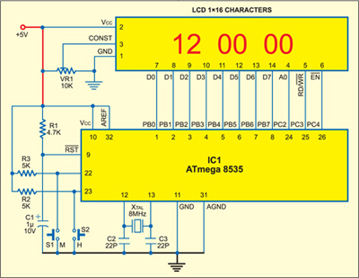
A crystal of maximum 16MHz or 8MHz frequency can be connected across pins 12 and 13 of ATmega8535 or its low-voltage version ATmega8535(L), respectively. Pin 9 serves as the active-low reset pin.
The non-volatile program and data memories built into ATmega8535 are:
1. 8 kB of self-programmable flash for storing the software code of the application program.
2. 512 bytes of SRAM, which is a read/write memory.
3. 512 bytes of EEPROM for storing the data. Unlike the flash memory, it can be accessed in a program for writing and reading.
Programming the on-chip code/program memory
The on-chip flash memory is programmed by pulling up the reset pin and sending data through pins 6 (MOSI) and 7 (MISO), and pin 8 (SCK), which is used for clocking the the code data into the flash memory. This is accomplished by the host computer by sending appropriate instructions and the code bytes; data verification is done by reading the flash memory and comparing it with the original code data. Writing the lock bits to prevent reading of the code in the chip is accomplished through the instructions and the relevant data.
For using the AVR device, these instructions are built into the ATPROG program (explained in Part I), which is run on the host PC.
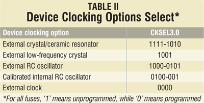
Selection of clock. There are some additional fuse bits, which can be programmed for some extra operational functions. Note that the AVR device, as shipped, is preset to work at 1 MHz with its internal oscillator. If you want to use an external crystal, say, of 8MHz frequency, you have to exercise this option by programming the fuse bits accordingly. A fuse bit is just like a flash code memory location.
The CKSEL fuse bits can be programmed to select the desired crystal. The device clocking options are selectable by Flash Fuse bits as shown in Table II. The clock from the selected source is input to the AVR clock generator and routed to the appropriate modules.
Since the default oscillator is 1MHz, unless we set the CKSEL bits to an appropriate value, the external crystal on pins 12 and 13 will not function for ATmega8535.
Programming the fuse bits. The fuse bit programming option is available on the screen when the AT-PROG is run on the PC. When this option is selected, it pops up a menu of its own. On this menu, you can write the necessary code for CKSEL programming. (Details of programming the fuse bits, lock bits and other options like boot memory option are given on pages 236 and 252 of the ATmega8535(L) manual provided in the EFY-CD of Nov. 2005.)
Internal registers. Six of the 32 registers can be used as three 16-bit indirect address register pointers for data space addressing, enabling efficient calculations. One of three address pointers (X, Y and Z registers, described under ‘register operations’ section) is also used for table look-up.
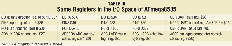
The I/O memory space contains 64 addresses for CPU peripheral functions like control registers, timers/counters and analogue-to-digital converter (ADC). It can be accessed directly or as the data space locations following those of the register files, i.e., after ‘20H’ and up to ‘5FH.’
The memory space contains important registers for use in interrupt selection, timer control, UART, SPI interface, watchdog and reset selection modes, etc. Table III shows the exact addresses of these I/O registers.
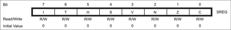
The bit description for the status register (SREG) is shown in Fig. 12.