


Here is a microcontroller based wireless equipment controller that can switch on or switch off up to four devices at a desired time interval set by the user in the transmitter. The devices can be controlled remotely from a distance of up to 30 metres from the transmitter. In the transmitter, an LCD module is used to show the device numbers and preset control time for the devices (00 to 99 seconds). Concepts of wireless RF communication and automation with AT89C51 microcontroller are used here.
The system is small, simple, cost-effective and good for wireless control of home appliances or industrial instrumentation.
Block diagram

The system comprises a transmitter and a receiver as described below.
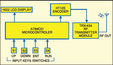
Transmitter section. Fig.1 shows the block diagram of the transmitter section.
Four pushbutton switches (S1 through S4) are used as inputs to select the devices and set the time-out in the transmitter section. These are designated as up, down, enter and run keys, respectively. The time-out data is transferred over the RF wireless link to the receiver section.
The 8-bit AT89C51 microcontroller is the main controlling part of the transmitter section. It is connected to the LCD module, input switches and encoder IC (HT12E). The device control program is stored in the memory of the microcontroller to control the devices as per the time-out settings done through input switches S1 through S4.
A two-line, 16-character LCD module shows the status of the main program that is running inside the microcontroller.
The HT12E is an 18- pin DIP package encoder IC that encodes 4-bit data and sends it to TRX-434 RF transmitter module.
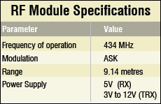
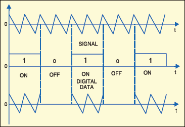
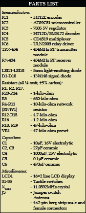
The TRX-434 RF transmitter module uses a digital modulation technique called amplitude-shift keying (ASK) or on-off keying. In this technique, whenever logic ‘1’ is to be sent, it is modulated with carrier signal (434MHz). This modulated signal is then transmitted through the antenna. The waveforms in Fig. 2 depict the ASK concept. The main specifications of the RF module are shown in the table.
Receiver section. Fig.3 shows the block diagram of the receiver section.
The 12V DC supply, used along with a 5V regulator, can be provided by a 12V battery or power adaptor.
The RX-434 radio receiver module receives the ASK signal from TRX-434. The HT12D decoder demodulates the received address and data bits. IC CD4519 is a quadruple two-input multiplexer that selects the appropriate data bits to control the devices.
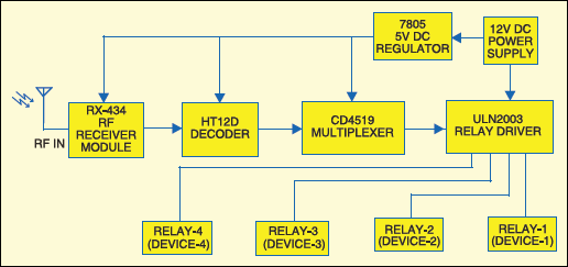
Fig.3: Block diagram of receiver section for wireless equipment control
The ULN 2003 relay driver consists of seven npn Darlington pairs that feature high-voltage outputs with common-cathode clamp diodes for switching the inductive loads. The collector-current rating of a single Darlington pair is 500 mA.
Circuit description
Transmitter circuit. Fig.4 shows the transmitter circuit. The microcontroller reads the input data from switches S1 through S4 at its port-2 pins 21 through 24 and displays it on the LCD. Port 3 provides read data to the encoder IC HT12E at pins 10 through 13. The microcontroller is programmed to control input and output data.
When the push button switches (S1 through S4) are open, logic ‘0’ is constantly fed to the respective port pins of the microcontroller. When any of the buttons is pressed, logic ‘1’ is fed to the respective port pin of the microcontroller.
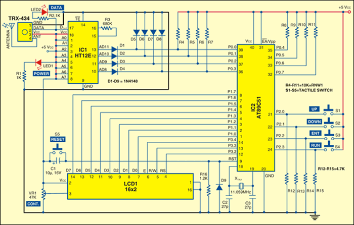
The device control program stored in the memory of the microcontroller activates and executes as per the functions defined in the program for respective input switches.
Data inputs AD8 through AD11 (pins 10 through 13) of HT12E are connected to the microcontroller. Pins 1 through 8 (A0 through A7) of the IC are address inputs. Shorting them address pins using switches to either Vcc or Gnd enables different address selections for data transmission. Here we have connected them to 5V. Since address pins are connected to 5V, the address is set to 255d (in decimal). If you were to connect all the address pins to ground, the address would be 000d. Thus there are 256 possible addresses available. So you can set up switches to control one or more of the encoder address pins.
Pin 14 is a transmit-enable (TE) input pin. The encoder will send data only when pin 14 is connected to ground. Whenever a button is pressed, logic ‘0’ is sent to this pin through the microcontroller, thus activating it and enabling transmission.
Pin 17 is the data-out (Dout) pin that sends a serial stream of pulses containing the address and data. It is connected to the data input pin of the TRX RF module.
The time-out control is set using input keys S1 through S4 to turn on/off the devices at predetermined time. The default time for all the devices is ‘00’ seconds. So using ‘up’ key you can increment time by one second, and using ‘down’ key you can decrement time by one second down. At the same time, the LCD module shows the current status of increments and decrements.
When the time-out for a device is set, press ‘ent’ key so that the program control transfers to the next device for time-out settings. In the same way, the remaining three time-out settings must be done before pressing ‘run’ key. When ‘run’ key is pressed, it executes the device control program subroutine in the microcontroller and the program automatically collects the time-out information entered by the user and sends the processed data to encoder IC HT12E. The encoder IC sends the data to Din (pin 2) of the RF transmitter module. The data is transmitted by the TRX-434 module to the receiver section through the antenna.
Receiver circuit. Fig. 5 shows the receiver circuit. The RF receiver (RX- 434) module can receive the signal transmitted by the transmitter from a distance of up to 9 metres (30 feet). The range can be increased up to 30 metres using a good antenna.
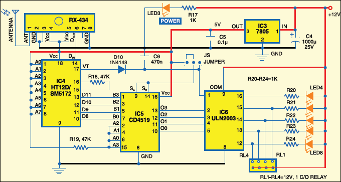
Dout pin of RX-434 RF module is connected to Din pin of decoder IC HT12D (IC4). Din pin of IC4 receives address and data bits serially from the RF module. Decoder IC4 separates data and address from the received information. It accepts data only if the received address matches with the address assigned to encoder IC1 (HT12E). We have used ‘1111’ as the permanent address for communication. Pins 1 through 8 of IC4 are address pins and therefore 256 possible addresses are available. The address on the encoder and decoder ICs must match for the data to be valid.
The HT12D decoder receives serial addresses and data from the encoder that are transmitted by a carrier signal over RF medium. The decoder compares the serial input data three times. continuously with its local addresses. If no error or unmatched codes are found, the input data codes are decoded and transferred to the output pins. VT pin (valid transmission) goes high to indicate a valid transmission. The HT12D provides four latch-type data pins whose data remains unchanged until new data is received.
Data pins D8 through D11 (pins 10 through 13) of the decoder send 4-bit data to CD4519 multiplexer IC5.
CD4519 multiplexer. This IC provides four multiplexing circuits with common select inputs (SA and SB); each circuit contains two inputs (An, Bn) and one output (On). It may be used ton select 4-bit information from one of the two sources.
There are eight input lines (A0 through A3 and B0 through B3), of which four (A0 through A3) are permanently connected to Vcc through resistor R19, while the rest four (B0 through B3) are connected to the data output lines of the decoder (IC4).
The select inputs can be connected to either Vcc or VT pin (pin 17) for latch or momentary mode-selection section. Jumper switch (Js) is used to select between latch and momentary operation. When latch mode is selected, data present at the output pins is latched, i.e., they remain the same and the respective relay energises until the next change is made in the mode selection. When momentary mode is selected, data present at the output pins is available as long as VT pin remains active-high. As soon as VTpin becomes active-low, the respective relay de-energises.
The latched output data from multiplexer CD4519 is fed to relay driver IC ULN2003, to control up to four devices through the relays (RL1 through RL4). VT pin is connected to LED4 through IC6 to indicate the status of VT signal when it is active-high.
Software program
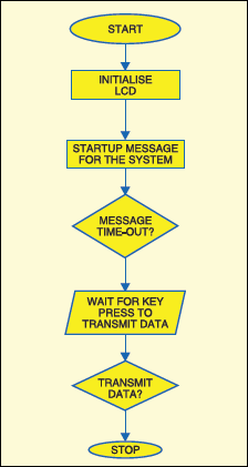
The software flowchart programmed in the microcontroller of the transmitter section is shown in Fig. 6. It is written in Assembly language and compiled using ASM51 software to generate the hex code. The hex program can be burnt into the AT89C51 microcontroller by using any standard programmer available in the market. We have used TopView programmer from Frontline Electronics to program the microcontroller.


good,,
What do you use to design the circuit? is Proteus ?