


Introduction
When we are experimenting with AM receivers for LW, MW and SW we are in need of high impedance analog probe with low input capacitance, e.g. well below 20pF.
The required input impedance from the probes at low frequency is usually 1MOhm or above.
Most of the low-cost passive probes for oscilloscopes are having input capacitance well above 100pF.

If we include the input capacitances of the oscilloscope the total capacitance will become even more.
The bandwidth of these low-cost passive probes is usually limited to 1-2MHz and they cannot be connected in parallel of the LC networks in the AM receivers because they will change significantly the parameters of these networks.
Description of the circuit for Low-Cost Dual Channel Active AC Analog Probe
Figure 1 is showing the circuit of very simple and low-cost dual channel active AC probe.
The probe can be used for oscilloscopes, multi-meters or other analog measurement equipment.
The probe can be implemented in small PCB.
When needed during the tests and adjustment the inputs of the probe can be soldered to the LC networks with very short conductors, e.g. with length of 3-4 cm.
Most of the oscilloscopes are with two channels and we are in need of two channels active probes with common ground and common power supply.
The input resistance of the probe at low frequency is determined mainly by the resistors R3 and R4 and is around 10Mohm in that case.
At high frequency, the input impedance is determined by the total input capacitance of the probe.
With careful implementation and appropriate JFETs the input capacitance can be below 20pF.
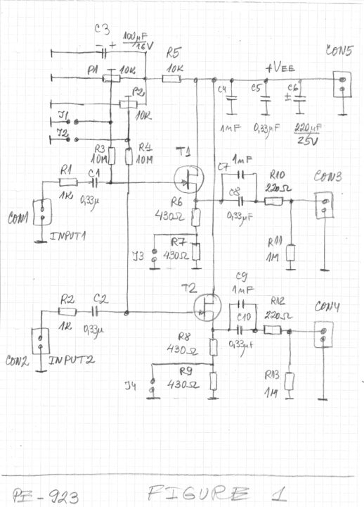
T1 and T2 should be transistors with the guaranteed low noise level and low input capacitance.
In that case the transistors are PN4391, PN4392 or PN4393 with input capacitance of typically 14pF.
Another appropriate transistors are J201, J202, J203, 2N5457, 2N5458, BF245 (NF=1.5dB), etc.
High frequency JFETs in small cases are preferred but they are having usually higher price.
It is important that the voltage between the drain and the source of T1 and T2 should be around half of the power supply.
The adjustment is made with the resistors R6, R7, R8, R9 and jumpers J3 and J4.
The circuit with R5, P1, P2 and C3 are used for adjustment of the applied to the gates of the JFETs offset voltages.
These components are not obligatory.
If omitted the jumpers J1 and J2 should be closed and R3 and R4 are connected to the ground.
The gain of each of the channels is slightly below unity but that is not important in most of the cases.
Most of the oscilloscopes are having reference source for test square signal that can be used for measurement of the gain and evaluation of the probe.
The circuit will start to work immediate after the proper montage is done.
The circuit does not require any special adjustment.
If used jumpers J3 and J4 and potentiometers P1 and P2 are set in order to obtain the best performance of the probe.
After proper implementation the probe can have bandwidth above 10MHz with signal generator with low output impedance.
The power supply should be 9V or above and is limited only by the transistors and capacitors.
The preferred power supply is from dry battery or rechargeable battery.