
The real world embedded systems are controlling DC motors, stepper motors, electromagnetic relays, incandescent lamps, powerful LEDs, displays, inductors, transformers, long cables, etc.
On the market we can find large variety of kits with embedded MCUs, DSPs, MPUs, etc. They are very useful for studying the operation of the integrated circuits on the board of the kit and for building prototypes of real embedded systems.
But two major problems are:

- Most of the kits cannot drive directly heavy loads
- The power supplies of the kits (if any) are not capable of providing power for heavy loads.
The parallel/printer port of the PC is still representing interest to control real world applications. But that port has the limitations of most of the kits stated above.
That sort paper is presenting one possible solutions for both problems. The solution can work with embedded kits with MCUs, MPUs and DSPs. Also the solution will work with printer port of the PC and with any parallel interface providing TTL/CMOS compatible signals.

Description of the circuit
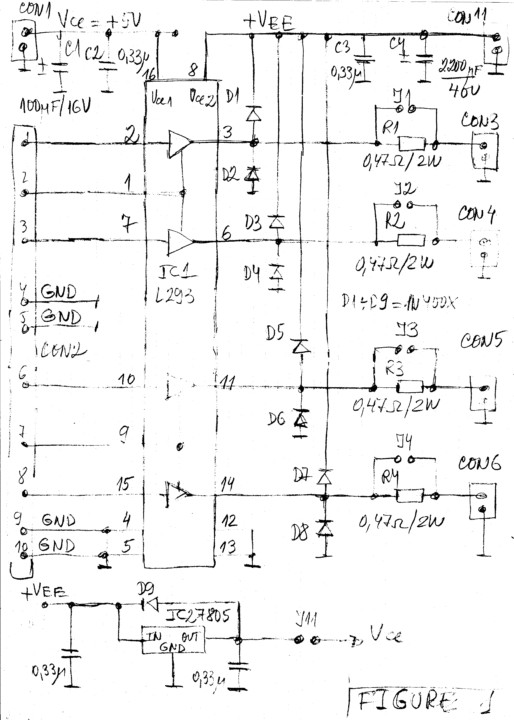
The circuit diagram of both parts of the multi-channel hardware driver for power loads is shown on Figure 1 and Figure 2.
Both parts are independent peripheral drivers with many configurations capable of solving a lot of peripheral tasks. It is preferably to implement both parts on single PCB, but if not possible two separate pcb can be used – one for figure 1 and second for figure 2. The part on figure 1 is built around the quadruple driver L293 or other pin to pin compatible digital driver.
L293, L293B and L293D are widely used quadruple half-H drivers. The drivers in these integrated circuits (ICs) are non-inverting. The ICs are produced in DIP16 and they have two powers supplies. The first is Vs for the peripherals and the second is Vss for the internal logic of the IC.
The power supply Vs (also called Vcc2) is from Vss up to 36V. Vss (sometimes named Vcc1) is from 4.5V up to 7V. The parameters of the ICs are guaranteed at Vcc1 = 5V and Vcc2 = 24V (always Vcc2>=Vcc1).
The voltage drop on the output driving transistors is around 1V at 0.5A and 1.5V at 1A. The peak output current is 2A for L293 and 1.2A for L293B. L293 can provide continuously up to 1A per channel and L293B can source and sink up to 600mA. The driver on Figure 1 has the following possible configurations:
- Four independent digital drivers
- Two, three or four digital paralleled drivers.
In paralleled configuration of the drivers the jumpers J1 to J4 should be open and we should verify that all drivers are providing similar currents.
- One or two bridged configurations for the outputs.
We can use also paralleled drivers in bridged configuration. In all configurations the inputs and the outputs of L293 should be properly wired with external connections. That part of the board has regulator 7805 which can provide +5V for L293 and for the kit with MCU if needed.
The +5V from 7805 is available on the connector CON1 when the jumper J11 is closed. 7805 should be mounted on heat-sink with thermal resistance below 28C/W. L293 also may require proper heat sink as described in the data sheet. The connector CON2 is for the signals from the MCU, kit with the MCU or from the printer port of the PC.
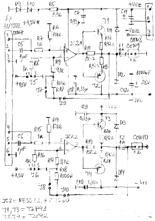
The connectors CON3 to CON6 are for the peripheral devices. The connector CON11 is for the power supply for the output peripheral drivers in L293. The second part of the board is given in Figure 2.
Both parts of the board are completely independent with the exception of the ground line. They can have independent and different power supplies. The second part of the board is built around dual operational amplifier (OA) as NE5532 or MC4560 and four transistors.
It has two independent channels. The signals from the MCU are applied on the connector CON7. The bipolar power supply is applied on CON8. The full power supply range of the OA is allowed on CON8. Both channels can work in the following modes:
1/ Dual DC analogue amplifier for the signals applied on pin 1 and pin 4 of the connector CON7.
In that application:
- the jumpers J5 and J6 are in position 3,
- the jumpers J9 and J10 are closed,
- the jumpers J7 and J8 can be open or closed (preferably closed).
2/ Dual AC analogue amplifier for the signals applied on pin 2 and pin 5 of the connector CON7.
In that application:
- the jumpers J5 and J6 are in position 3,
- the jumpers J9 and J10 are closed,
- the jumpers J7 and J8 can be open or closed (preferably closed).
Now both channels can work as mono or stereo audio amplifiers or as general purpose AC amplifiers with output currents up to around 1A
If the jumpers J7 and J8 are closed the gain is around 10.
When the jumpers J7 and J8 are open the gain is around 1000.
3: Dual digital driver with threshold of 1.5V for the DC or AC signals applied on pin 1 and pin 4 of the connector CON7.
In that application:
the jumpers J5 and J6 are in position 1, you can have any combination of open and close jumpers J9/J10 and J7/J8 according to the needs. Both channels from Figure 2 can work in the same or in different modes.
T1/T3 are TIP41 and T2/T4 are TIP42.
It is possible to use Darlington transistors as TIP122/127 but we should pay attention to the maximal output currents. Transistors should have at least small individual heat sinks with thermal resistance below 28C/W (bigger heat-sinks are preferred).
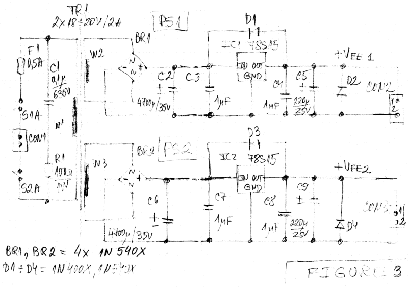
The power supply and its configurations
The board described in Figure 1 and Figure 2 needs external power supply (PS). We should use single power supply for L293 and dual power supply for the section with the OAs. One possible solution for the power supply is shown on the Figure 3. The power supply consists of two identical sections PS1 and PS2 with fixed regulators 78S15 (+15V/2A)
We may use standard 7815 providing +15/1A.
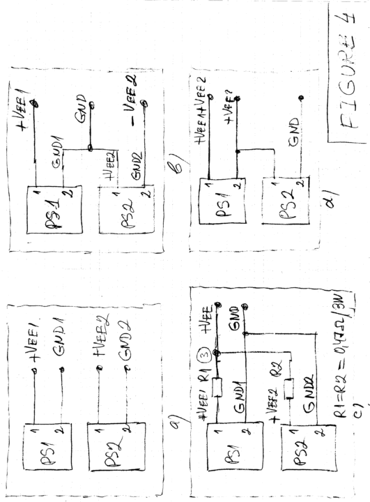
The regulators have to be mounted on two separated heat-sinks with thermal resistance below 15C/W. Figure 4 is showing four different configurations of that power supply.
* Figure 4a – usage as two separated power supplies with separated output lines and common transformer.
* Figure 4b – usage as power supply providing +Vee1 = +15V and –Vee2 = -15V
* Figure 4c – usage as two paralleled power supplies with common output lines.
In that case we should use equalization resistors with usual value 0.47-1Ohm/3-5W. The total output current from the joined output in point 3 with 78S15 is up to 4A and with 7815 is up to 2A.
* Figure 4d – usage as one power supply producing +Vee2 = +15V and +Vee1+Vee2 = +30V
Conclusions
That short paper is presenting multi-channel hardware driver for embedded systems. The board can be used with most of the kits with MCUs, MPUs and DSPs and with the printer port of the PC. The boars has many configurations can solve a lot of peripheral tasks.
Before each usage the jumpers should be properly installed.
a: two separated power supplies (PS1 and PS2) with separated output lines and common transformer.
b: power supply providing +Vee1 = +15V and –Vee2 = -15V
c: two paralleled power supplies with common output lines.
d: one power supply producing +Vee2 = +15V and +Vee1+Vee2 = +30V