


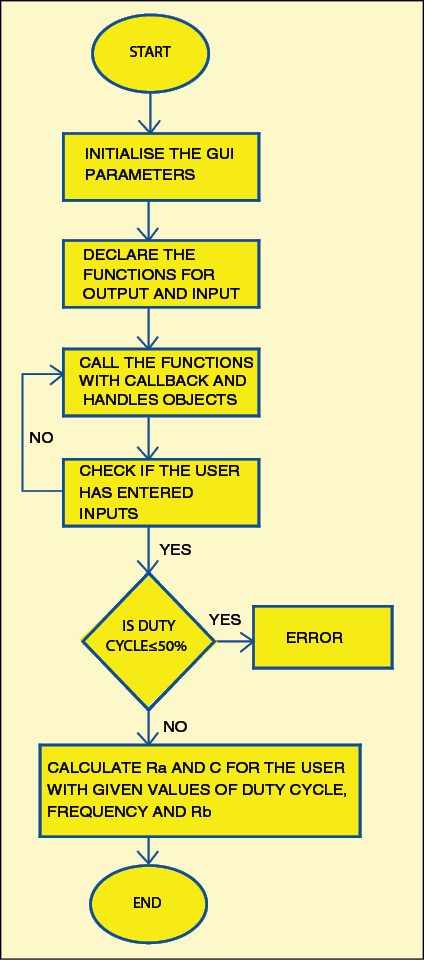
Presented here is a Matlab program to design an astable multivibrator of desired frequency and duty cycle using a 555 timer. The aesthetic graphical user interface of the program helps you quickly calculate the values of timing components for your design requirements.
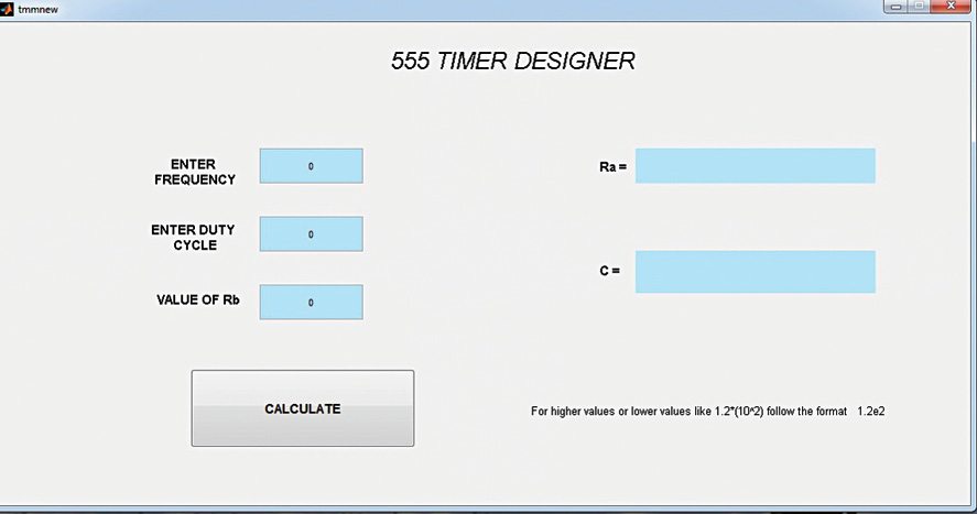
Fig. 1 shows the graphical interface where the desired frequency and duty cycle can be directly entered to calculate the value of timing components by the program.
Let us first discuss the basic functionality of a 555 timer to better understand how the Matlab program works.

555 timer
The 8-pin 555 timer is one of the most popular ICs in the electronics world. With just a few external components it can be used to build amazing timer, pulse generator and oscillator applications. A popular version is NE555, which is suitable in most cases where a ‘555 timer’ is specified.
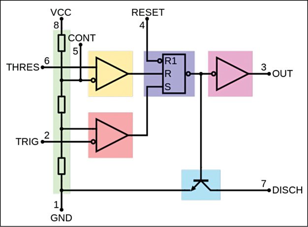
Fig. 2 shows the internal diagram of a 555 timer to help you understand its pins’ functionalities:

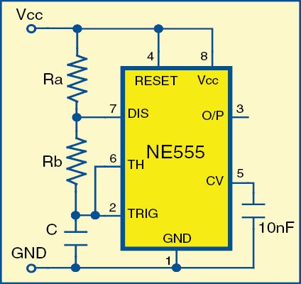
Pin 1: Ground terminal. All the voltages are measured with respect to this terminal.
Pin 2: Trigger terminal. This pin is an inverting input to comparator-2. It is responsible for transition of the output of flip-flop from set to reset. The output of the timer depends on the amplitude of the external trigger pulse applied to this pin.
Pin 3: Output terminal. The output of the timer is available at this pin.
Pin 4: Reset terminal. To disable or reset the timer, a negative pulse is applied. When this pin is not to be used for reset purpose, it should be connected to +Vcc to avoid any possibility of false triggering.
Pin 5: Control voltage terminal. The function of this terminal is to control the threshold and trigger levels. Thus either the external voltage or a potmeter connected to this pin determines the pulse width of the output waveform. The external voltage applied to this pin can also be used to modulate the output waveform. When this pin is not used, it should be connected to ground through a 0.01µF capacitor to avoid any noise problem.
Pin 6: Threshold terminal. This is the non-inverting input terminal of comparator-1. It compares the voltage applied to the terminal with a reference voltage of 2/3Vcc. The amplitude of the voltage applied to this terminal is responsible for set state of the output of flip-flop.
Pin 7: Discharge terminal. This pin is connected internally to the collector of the transistor; mostly a capacitor is connected between this terminal and the ground. It is called discharge terminal because when the transistor saturates, the capacitor discharges through the transistor. The capacitor charge/discharge rate is determined by the external resistors.
Pin 8: Supply terminal. A supply voltage of +5V to +18V is applied to this terminal with respect to the ground (pin 1).
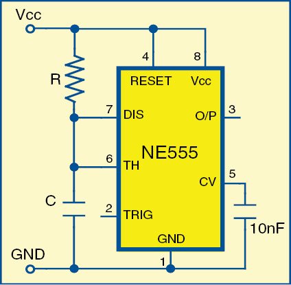
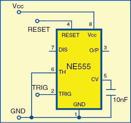
There are literally thousands of different ways in which the 555 timer can be used in electronic circuits. In almost every case, however, the basic circuit is wired in one of the three operating modes: