 The most frequently used device in electronic workshops and laboratories is a universal power supply that provides a variable, fluctuation-free output. Here we present a variable power supply with digital control that is simple and easy to construct.
The circuit is built around an adjustable 3-terminal positive-voltage regulator IC LM317, CMOS decade counter IC CD4017, timer IC NE555 and 3-terminal fixed negative-voltage regulator LM7912.
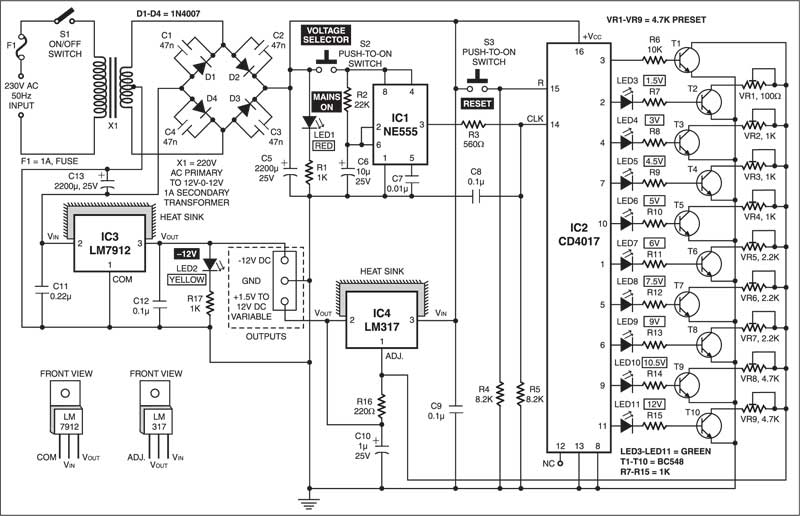
The AC mains supply is stepped down by transformer X1 to deliver a secondary output of 12V-0-12V AC, 1A. The output of the transformer is rectified by a full-wave rectifier comprising diodes D1 through D4. Capacitors C1 through C4 are connected in parallel to rectifier diodes to bypass undesired spikes and provide smooth and fluctuation-free power. Capacitors C5 and C13 are used as filters to eliminate ripple. Here both negative and positive half cycles are used to obtain positive as well as negative DC output. LED1, along with current-limiting resistor R1, is used for mains ‘on’ indication.
Variable power supply circuit

Timer IC NE555 (IC1) is wired as an astable multivibrator. It generates clock pulses when switch S2 is pressed. The output of IC1 is connected, via an RC network, to the clock input of counter IC CD4017 (IC2).
IC CD4017 is a decade ring counter. Each of its ten outputs goes high one by one when a clock pulse is received. The outputs of IC CD4017 are connected to the bases of transistors T1 through T10, respectively, as shown in the figure. LED3 through LED11 are used here to indicate the voltage levels. The collectors of transistors T2 through T10 are connected to presets VR1 through VR9, respectively, which are used to set the output voltage.
Adjustable voltage regulator IC LM317 (IC4) develops 1.25V nominal reference voltage (VREF) between its output and the adjustable terminal. The reference voltage appears across resistor R16. When the voltage is constant, a constant current flows through one of the output-setting variable resistors (VRset, VR1 through VR9), giving an output voltage at pin 2 of IC4 as follows:
VOUT=1.25(1+VRset/R16).
Presets VR1 through VR9 are adjusted to get the desired output voltage. The collector of transistor T1 is directly connected to ADJ terminal (pin 1) of IC4, so the output voltage of IC4 will be the voltage across fixed resistor R16, which is equal to 1.25V. When switch S3 is pressed, pin 3 of IC2 goes high and the output voltage becomes 1.2V.
Circuit operation
When switch S2 is pressed, the output of IC1 goes high. As a result, the outputs of IC2 go high one by one as a ring counter. Since presets VR1 through VR9 are connected at the collectors of transistors T2 through T10, respectively, different output resistances appear between the adjustable and ground terminals of IC4, resulting in different output voltages. By using a properly calibrated digital multimeter you can easily adjust the presets to obtain 1.5V to 12V.
A fixed, negative 12V DC can be obtained by using fixed, negative-voltage regulator IC LM7912 (IC3). Thus the power supply unit can be used for circuits requiring both negative and positive DC voltages.
When CD4017 is reset by pressing switch S3, the output voltage becomes 1.2V and all the voltage-indication LEDs turn off.
Assemble the circuit on any general-purpose PCB and enclose it in a suitable cabinet. Use suitable heat-sinks for regulators IC3 and IC4. Since pin configurations of the regulators are different, never fix both regulators on the same heat-sink. For S2 and S3, using microswitches will enhance the beauty of the unit. LED2 is used to indicate the negative 12V DC voltage.
More interesting projects available here.


Very nice and cute one. Can I get a PCB layout? If so, Please mail me at [email protected].
Have a nice day!
Thanks for the feedback! PCB layout of this circuit is not available, sorry.
Can I get a PCB layout? If so, Please mail me at [email protected]
Very nice Project. Can I get a PCB layout on my mail ID: [email protected]
Can you please tell me what’s the purpose of the negative 12 volt supply in this project ?
Very nice Project. Can I get a PCB layout on my mail ID: [email protected]
Very nice Project. Can I get a PCB layout on my mail ID:
[email protected]
Very functional and practical project, congratilations.
If possible can i get PCB layout ?
my mail ID is [email protected]
Thanks
Please send me the PCB layout on my e mail id [email protected]
Great creation! Please kindly email me the PCB via [email protected]. Thank you so much in advance!
Very nice , good job.. Sir please kindly email me the pcb layout on my email I’d ([email protected]) please please please.
PCB layout is not available for this circuit, sorry.
why is everyone asking for the pcb circuit layout. great instructions! thank you 🙂
PCB layout is not available for this circuit,
Thx
Very nice Sir. I’m appreciate of your
Please kindly send me PCB layout if possible
Email:- [email protected]
I’m trying to build this circuit but I do havce a question, what are the transistors T1 to T10 ?
I’ve read the entire text but it doesn’t mention what transistors are used.
The collectors of transistors T2 through T10 are connected to presets VR1 through VR9, respectively, which are used to set the output voltage