

With the advent of technology in the growing US$ 5 billion field programmable gate array (FPGA) market, the board and the system computing shrank from a single-board computer to a system on chip (SoC). Developing a new mask, or circuit pattern, to upgrade a single chip can cost US$ 2 million to US$ 5 million.
As a consequence of missing product cycles, issues related to technology or design come up that cost a dear to the revenues. End users often have to replace equipment or endure sub-optimal performance because of unanticipated in-field conditions. Modems need to be reconfigured for various processing schemes of communication and digital signal processors (DSPs) or other processing tasks that require hardware acceleration.
With these reasons, FPGA paired with a custom chip is a great idea. The ultimate point of making a custom chip is to integrate and consolidate. Essential features of the FPGA are good performance, smallest form factor, lowest power consumption and lowest bills of material (BOM) cost.

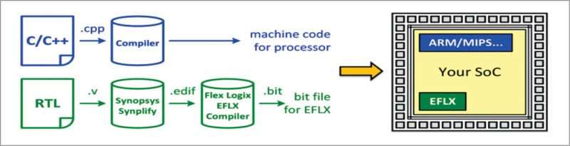
 This technology puts some FPGA fabric in the custom chip design. Customers do not require any FPGA expertise to use the technology. If one customer needs pins for X and another customer needs for Y, he or she can do it in-code with existing chips. To enable customers to do hands-on evaluation, embedded flexible (EFLX) will make available free, under the encrypted Verilog model, LIB, LEF and detailed datasheet of EFLX core.
EFLX blocks can be used anywhere in the chip—connected to RAM and input/output (I/O), used in the data path or on the processor bus. But FPGA companies do not offer their fabric as intellectual property. FPGAs require many metal layers to achieve routability, which is needed to make these useful. If the device does not include many layers, it would take a major and expensive upgrade of design to handle the overhead of adding conventional FPGA fabric to the mix.
But the so-called EFLX technology is based on programmable logic with RTL reconfigurability. EFLX technology allows SoC designers to embed FPGA into complex chip designs. Applications such as encryption, networking and signal processing require blocks of RAM to be integrated into the FPGA to provide fast local memory to implement buffers, scratchpads, FIFOs and other low-latency memory that improves performance.
EFLX is a fully-functional FPGA. Instead of existing in systems as a standalone chip, it is integrated into communications chips, microcontrollers (MCUs) and other devices. The technology is scalable for larger designs. Larger EFLX cores could easily be developed to support array configurations over 300k gates.
EFLX has developed a new and novel type of hierarchical interconnection network that can cut interconnect resource requirements by 50 per cent or more, reducing the number of metal layers required. At the same time, the more efficient interconnect reduces power consumption, improves performance and makes timing closure easier. Hardware design is fast but fixed, while software like operating systems or apps can be easily changed. It provides licences for its technology to chip makers who can embed EFLX hardware into their own designs. Wireless networks could get speed upgrades sooner, or Internet services like search engines could be upgraded with new features.
Typical applications include fast control logic, intelligent I/O crossbars, customisable DSP accelerators, logic blocks to support many market segments or customers with a single chip, reconfigurable base-station digital front-ends, programmable parsers, reconfigurable protocols and more. EFLX can provide a ton of I/Os—632 per direction per tile in a 7 x 7 array that adds up to big numbers even after tile-to-tile and memory interconnects. In the MCU segment, EFLX blocks can be configured as something that amounts to a smart crossbar.
EFLX, a fully-functional FPGA
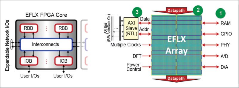
EFLX FPGA has parallel data paths running vertically and interfacing to peripherals laterally such as the advanced extensible interface AXI Slave, which connects to ARM advanced MCU bus architecture. Basic part is an FPGA; interconnect and I/O block is called EFLX-2.5K when built on TSMC 28HPM. The 28nm high-performance mobile (HPM) computing provides high performance for mobile applications to address the need of applications requiring high speed. Such technologies can provide the highest speed among 28nm technologies. It gives implementer 2520 LUTs, 5040 flip-flops, eight clocks, 632 inputs and 632 outputs.
The second variant is called EFLX DSP core, and its main addition is a DSP block.
EFLX blocks can be used anywhere in a chip for connection to RAM and I/O, in the data path or on a processor bus. It can integrate any kind of RAM of any width, size, having single or dual port, ECC, parity or neither. Memory can be put between cores and controlled with unused I/O.
EFLX memory compiler maps RTL code onto the array including RAM. EFLX blocks are programmed with RTL. Both architectures can be tiled together in up to a 7 x 7 array, and, if needed, provide GDS, LIB, LEF and Verilog files. The incremental die cost is less than five cents per k-input-look-up tables (k-LUTs), which is much less than packaged FPGAs.
If memory is needed, interconnects between the tiles can have DRAM blocks added to these. Instead of wiring up I/Os from one tile to the next directly, memory is placed between tiles, and I/Os on the periphery of the tile group take over I/O duties for the entire set.
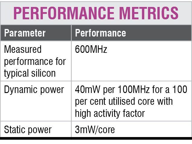
28nm is the first generation that foundry industry starts to use high-k metal gate (HKMG) process, which represents TSMC. Still, poly/oxnitride process is offered to meet customers’ time-to-market need. It is ideal for low standby power applications such as mobile baseband. In a 28nm process, fast control logic can run at 525MHz or more, and pipelined finite impulse response filters (FIRs) can run up to 450MS/s or faster.
In 40nm, multiple speed/power tradeoffs are supported to address almost all possible requirements. The 28nm low-power with high-k metal gates (HPL) technology adopts the same gate stack as HP technology while meeting more stringent low-leakage requirements with a trade of performance speed.
The 28nm family also provides a wider variety of metal options to support a broad range of product applications for better trade-off between performance and density. It only requires six metal layers instead of the traditional ten or more in conventional mesh FPGAs, and offers 1.8 times higher logic density, thanks to optimised interconnect.
TSMC offers three processes at 28nm. These are 28LP, 28HP and 28HPL processes. Millions of production wafers have come out of TSMC’s 28nm processes. In TSMC, 28HPM/C fast control logic can run at 525MHz or more, and pipelined FIRs can run at 450MS/s or faster.
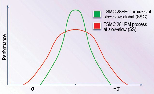
Designers can improve SoC performance by using global slow and fast (SSG, FFG) signoff corners. These are enabled by TSMC’s tighter process controls with 28HPC/HPC plus over 28LP/HP/HPL/HPM. Improved performance enables the use of lower-drive (smaller) logic cells to close critical-timing paths.
28LP process. 28LP process has 20 per cent speed improved over 40LP process at the same leakage/gate.
28HP process. 28HP process targets CPU, GPU, FPGA, PC, networking and consumer electronics applications. It supports 45 per cent speed improvement over 40G process at the same leakage/gate. With higher performance coverage, 28HPM is ideal for many applications in networking and high-end smartphone/mobile consumer products.
28HPL process and 28HPM. 28HPL process reduces both standby and operation power by more than 40 per cent. Compared with TSMC’s 28LP, 28HPC provides ten per cent smaller die size and more than 30 per cent power reduction at all levels of speed. A comprehensive 28HPC IP ecosystem is also built and compatible with 28HPM, accelerating time-to-market for customers. 28HPC is also ideal for many applications in mid- and mid-to-low end smartphones, tablets and mobile consumer products.
EFLX cores
EFLX core is memory type and needs to be TSMC 28HPC-compatible. TSMC provides high-performance compact mobile computing, the most energy-efficient and high-performance method of manufacturing for customers looking to tap chip area and power saving benefits of mid- to low-end SoC designs.
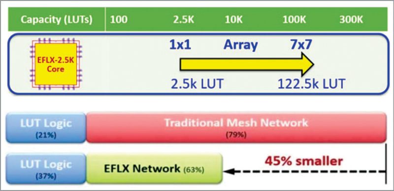
Architecturally, core tiles can be combined into arrays. For EFLX-2.5K, up to a 7 x 7 array is feasible for a total of 122.5k LUTs. This reminds of systolic arrays with multiple FPGAs of yesteryear, minus the nasty external chip-to-chip interconnect problems. EFLX tile array can implement an optimised data flow DSP pipeline, or multiple EFLX tiles could be scattered across functional blocks in an SoC.
EFLX cores are RAM based, which is programmed from RTL and is converted into a stream of configuration bits. Current technology is EFLX-2.5K core, available in TSMC 28nm HPM/C and packing 2.5k LUTs, as the name implies.
EFLX cores consist of individual 2500-LUT (lookup table) cores. These add less than 15 cents to the total manufacturing cost of a device. These cores can be integrated into multiple circuit blocks in the same design, or tiled together to create arrays of 7 x 7 or more EFLX cores for better performance.
EFLX cores come in two sizes, and each of those can be tiled together to make larger arrays of the FPGA fabric. EFLX logic core incorporates 40 multipliers-accumulators (MACs) with 22-bit inputs and 48-bit accumulation. The MACs can be combined for double the precision and pipelined for high throughput. These can also be used as complex-number MACs for certain DSP algorithms. With the same number of LUTs, EFLX is 1.8 times smaller in total area than the traditional mesh of FPGA.
Each EFLX core is divided into reconfigurable building blocks (RBBs), tuned for existing synthesis tools. This allows highly-optimised interconnect and logic placement. Any RBB can connect with another RBB, on the same EFLX tile or another tile in a connected EFLX array, up to a practical limit of 7 x 7 array size. With a single EFLX core, it is possible to implement valuable functions such as software-reconfigurable I/O pin-multiplexers and crossbars, reconfigurable fast control plane logic, reconfigurable multi-stage FIRs or the ability to change custom hardware accelerators post production.
Individual EFLX core tiles can be snapped together to form M x N arrays using the same EFLX network for interconnect, making the power of the concept clear. In addition to local memory, many applications also require DSP capability. Tiles with DSP emphasis or logic emphasis can be mixed and matched in an array for optimisation.
EFLX-100 core comprises three major blocks: RBBs of logic/DSP type, interconnect network and user I/Os. EFLX features full connectivity inside the core, and provides additional interconnects at the boundary to concatenate multiple cores via expandable network I/Os. Each core has an internal power grid (VDDH and VSS), which can be connected to the customers’ digital SoC power grid.
The core has power-control pins for power on and power gating, and includes configuration bits that are configurable via AXI, JTAG or a custom serial interface. On each side of the core there are two input clocks and two output clocks, which concatenate in EFLX arrays. Every LUT has an optional flip-flop at the output.
Additional logic implements carry chains for adders and comparators. Reconfigurable logic is interconnected by a reconfigurable interconnect, which allows any logic block to connect to any other. It also has patented interconnect that doubles density and only requires six or less routing layers for volume-chip compatibility.
EFLX-100 core is available in five different configurations and two nominal voltages, each optimised for different performance-to-power requirements for different target applications. Use of commercial synthesis tool chains also enables use of their other features including synthesis constraints and FPGA debug tools. The tools just need to know which tiles are being used and what arrangement we need to put these in (1×2, 2×2 and so on), let us say, to make up to 7 x 7 arrays of their 2500-LUT tile tailored for custom FPGA-in-a-chip.
EFLX-100 core is the ultimate in point-level reconfigurability where just a few gates are needed, and has targeted it for a mature TSMC 40nm LP/ULP process. Evaluation and prototyping of a single-core EFLX design gives customers the experience and insight to build flexibility into their RTL designs, even if the target application requires a larger EFLX array. EFLX cores available are TSMC 28HPM/C EFLX-2.5K core (either logic or DSP version) and TSMC 40ULP/LP EFLX-100 core (either logic or DSP version).
Benefits
EFLX cores allow a single SoC design to adapt to multiple requirements quickly using RTL re-configurability instead of locking in an SoC design with hard-wired logic, or trapping something deeply proprietary for a specific customer. These cores also allow field reconfiguration, which is essential for long-lifecycle devices.
EFLX makes the toolkit available to designers for post-production flexibility. By adding BRAM and DSP block RAM architecture, one can provide exactly the type and amount of memory an application requires. This flexibility is accomplished by inserting BRAM between EFLX logic cores, which tile together to make an array controlling these with otherwise unused inward-facing inter-tile I/Os.
External RAM is mapped and compiled onto the array. EFLX cores can be used to upgrade I/O protocols, change encryption algorithms to improve security, enable elements of software-defined radio or accelerate data centre algorithms like search.
Since EFLX core tiles are independent, these can be spaced apart, leaving room for external RAM integration between tiles. Semiconductor designers would have the ability to quickly upgrade their designs, equipment manufacturers would be able to modify product lines as required and end users would be able to optimise performance of their systems to address their own unique use cases and extend their product lifecycles. EFLX arrays could really help system-level SoC architecture.
Conventional IP model
EFLX supplies a full set of tools for populating the FPGA design. Adding a 2500-LUT core to a design should add only 15 cents to the total manufacturing cost of your device.
Benefits are board complexity, form factor, power consumption and performance. It also eliminates the need for all those external I/Os that would have connected your custom chip to the external FPGA and all PCB traces that would have carried those signals.
Fabric is the key to both performance and scalability. Addition of low-latency memory and signal-processing capabilities significantly increase the range of applications addressed by EFLX embedded FPGA-in-SoC architecture.
EFLX compiler
EFLX compiler with full timing files is available under a simple software-evaluation licence. This would enable you to determine area, performance, architecture and floor planning using EFLX-reconfigurable RTL. If you wish to proceed to design and build an evaluation chip, it would provide a fast-track licence for a single-core EFLX array for US$ 50,000. The licence would include full Verilog model, GDS-II, CDL, integration guidelines, EFLX compiler licence with full timing files and bit-stream generation.
Integration assistance will also be provided. To upgrade an EFLX FPGA, you would need to upgrade its RTL code, run it through Simplify Tool to produce an electronic design interchange format netlist and then use EFLX compiler to reconfigure the internal FPGA on the SoC. For such customers, the company has written its own compiler that allows easy upgrades in the field. The business plan and more-efficient FPGA architecture also reduce the number of metallisation layers to lower cost per gate.
Flow
- Make input RTL to see resources required, that is, LUTs, DSP blocks and RAM
- Configure EFLX array
- Select EFLX array size, optional DSP, type and amount of RAM, clocks and I/O configuration to connect EFLX array with the rest of the SoC
- Input RTL to see the worst-case path and frequency for target EFLX array/node
- Generate bit file that programs EFLX array in the SoC to execute RTL
The basic building block for implementing DSP functions is a pre-adder MAC EFLX logic core that incorporates 40 MACs with 22-bit inputs and 48-bit accumulation. The MACs can be combined for double the precision and pipelined for high throughput. These can also be used as complex-number MACs for certain DSP algorithms.
Trend setters
The three main market segments for EFLX core are networking, wireless/digital front-ends and microcontrollers (MCUs). With the sheer number of I/Os EFLX tile has, it can implement 256b or even 512b busses and put logic on the pins that need it.
Another useful feature of programmable logic is applicable to the wireless side of things, especially digital front-ends. If something changes or a hash/algorithm is blacklisted or cracked, you need not replace the entire device, just update it. In this space a little re-configurability goes a long way.
Applications
Application engineers who work on software-defined radio use FPGA fabric to swap among multiple modems on the fly. That is something they cannot accomplish easily with a stand-alone custom chip. In the video business, engineers could drive various display scales and resolutions with a single device by customising the FPGA fabric to match up to various display standards.
If your application requires compute acceleration, FPGA fabric could be reconfigured to implement various custom accelerators. But if your application requires custom hard logic that does not happen to be on those devices, EFLX will allow you to design those same benefits into your custom IC.
Enabling customers to customise and optimise
The big issue is not IP but tool chains, each of which may have a portfolio comprising hundreds and thousands of processor variations. In many cases, these variations involve relatively minor changes like pinouts. Incorporating even a single EFLX-100 core in each MCU could dramatically reduce the number of different MCU options. Also, the ability to customise the MCU’s abilities using programmable fabric may have tremendous implications with regards to implementing versatile nodes for use with the Internet of Things (IoT).
As SoC designs get more complex and masks cost millions of dollars, ICs and systems companies need to make their designs flexible enough to handle broader applications to generate more revenue and improve rate of interest, and to build the capability to upgrade critical RTL blocks to handle evolving standards and customer requirements. This flexibility enables new business models wherein system upgrades offering valuable new capabilities can be offered for a fee, or where one chip can be offered in several versions with different reconfigurable RTLs for different applications and priced to the value of each.
Architects, front-end designers and physical design teams need to become familiar with this new technology for applications from MCU to the IoT to networking and more. Evaluation and prototyping of a single-core EFLX design will give customers the experience and insight to build flexibility into their RTL designs, even if the target application requires a larger EFLX array.
V.P. Sampath is a senior member of IEEE and a member of Institution of Engineers India. He is a regular contributor to national newspapers, IEEE-MAS section, and has published international papers on VLSI and networks


